Nonvolatile semiconductor memory device having excellent charge retention and manufacturing process of the same

a semiconductor memory and charge retention technology, applied in semiconductor devices, digital storage, instruments, etc., can solve the problems of high device integration difficulty, data erasure operation speed improvement difficulty, etc., and achieve excellent adhesiveness and excellent productivity.

Inactive Publication Date: 2006-06-08
ASAHI GLASS CO LTD +1
View PDF11 Cites 95 Cited by
  • Summary
  • Abstract
  • Description
  • Claims
  • Application Information

AI Technical Summary

Benefits of technology

[0050] This construction, in a case of utilizing the eighth and sixteenth aspects of the present invention, enables to realize a nonvolatile semiconductor memory device in which the charge retention layer of the nonvolatile semiconductor memory device having the above-mentioned characteristics can be suitably formed, can be realized since the sput...

Problems solved by technology

This problem causes various problems in the characteristic of the above-mentioned nonvolatile memory devices, such that miniaturization or h...

Method used


Image

  • Nonvolatile semiconductor memory device having excellent charge retention and manufacturing process of the same
  • Nonvolatile semiconductor memory device having excellent charge retention and manufacturing process of the same
  • Nonvolatile semiconductor memory device having excellent charge retention and manufacturing process of the same

Examples


example 1

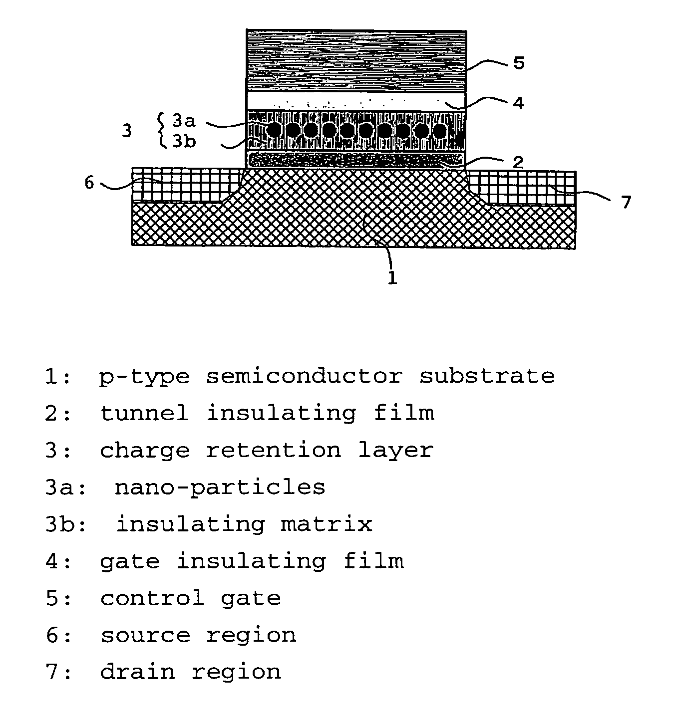
[0099] The nonvolatile semiconductor memory device of this Example will be explained, referring to FIG. 2. A tunnel insulating film 2 was formed on a p-type semiconductor substrate 1. The tunnel insulating film 2 was formed on the surface of the semiconductor substrate 1 by subjecting the semiconductor substrate to thermal oxidation at 800° C. and had a thickness of 5 nm.

[0100] Then a charge retention layer 3 constituted by an insulating matrix 3b containing nano-particles 3a, was formed so as to have a thickness of 5 nm by a capacitively coupled magnetron sputtering method as described below. Metal Co having a work function of 5.0 eV was selected for the nano-particles and amorphous SiO2 having an electron affinity of 1.0 eV for the insulating matrix. In the sputtering step, a target composed of a SiO2 target having a diameter of 3 inches (7.62 cm) and Co chips of 5 mm square placed thereon, was employed. The amount of the Co chips was adjusted so that the chips occupy 20% of the ...


PUM


Abstract

There has been a problem in conventional Si-type floating-gate type nonvolatile semiconductor memory devices that the charge retention characteristic is low due to insufficiently large electron affinity of Si, therefore improvement of the memory performances, such as scaling down of a memory cell and increasing operation speed, have been difficult to be achieved due to the essential problem. In order to solve the above problem, in the nonvolatile semiconductor memory device of the present invention, a material having large work function or large electron affinity or a material having a work function close to that of semiconductor substrate or of a control gate, is employed for a floating gate retaining charges. Further, an amorphous material having small electron affinity for an insulating matrix is used. Further, at a time of deposition of charge retention layer, the supply ratio of the nano-particle material and the insulating matrix material, such as the mixture ratio of materials of both phases in a target in a sputtering method, is adjusted. By these methods, the charge retention characteristic of the floating-gate type nonvolatile semiconductor memory device can be improved, and the above-mentioned problem of the nonvolatile semiconductor memory device can be solved.

Description

BACKGROUND OF THE INVENTION [0001] 1. Field of the Invention [0002] The present invention relates to a nonvolatile semiconductor memory device and its manufacturing process. In particular, the present invention relates to a structure in which particles with nano-scale consisting of at least one type of single-element substance or its compound are densely distributed in an insulating matrix. Further, the present invention relates to a nonvolatile semiconductor memory device having a charge retention layer with excellent retention characteristic by optimizing the work function or the electron affinity between the nano-particles and the insulating matrix, and by optimizing the distances between surfaces of adjacent nano-particles, and its manufacturing process realizing low cost and good reproducibility. [0003] 2. Discussion of Background [0004] Heretofore, as a recording medium in which a large amount of data can be memorized and rewritten, a memory device employing a semiconductor su...

Claims


Application Information

Patent Timeline
IPC IPC(8): H01L29/76
CPCH01L29/42332Y10S977/943
Inventor TAKATA, MASAAKIKOYANAGI, MITSUMASA
Owner ASAHI GLASS CO LTD
Why Eureka
Try Eureka