Methods and Structures to Produce a Strain-Inducing Layer in a Semiconductor Device

a technology of strain-inducing layer and semiconductor device, which is applied in the direction of semiconductor devices, electrical appliances, basic electric elements, etc., can solve the problems of impede the progress of particles, and achieve the effect of increasing stress and improving contact resistan

Inactive Publication Date: 2006-06-08
TAIWAN SEMICON MFG CO LTD
View PDF23 Cites 52 Cited by
  • Summary
  • Abstract
  • Description
  • Claims
  • Application Information

AI Technical Summary

Benefits of technology

[0002] Disclosed are methods for forming strain-inducing layers in semiconductor devices. Circuit elements are formed on a semiconductor substrate with conductive channel regions within the semiconductor substrate. Metal silicide contacts are formed on the semiconductor substrate and some are electrically connected to the channel regions. The metal silicide contacts provide an improved contact resistance relative to non-silicided metallization contacts. As disclosed herein, a strain-inducing layer can then be formed over the m

Problems solved by technology

Ideally, these moving charged particles would pass through the crystalline lattice of a semiconductor without any colli

Method used


Image

  • Methods and Structures to Produce a Strain-Inducing Layer in a Semiconductor Device
  • Methods and Structures to Produce a Strain-Inducing Layer in a Semiconductor Device
  • Methods and Structures to Produce a Strain-Inducing Layer in a Semiconductor Device

Examples


Embodiment Construction

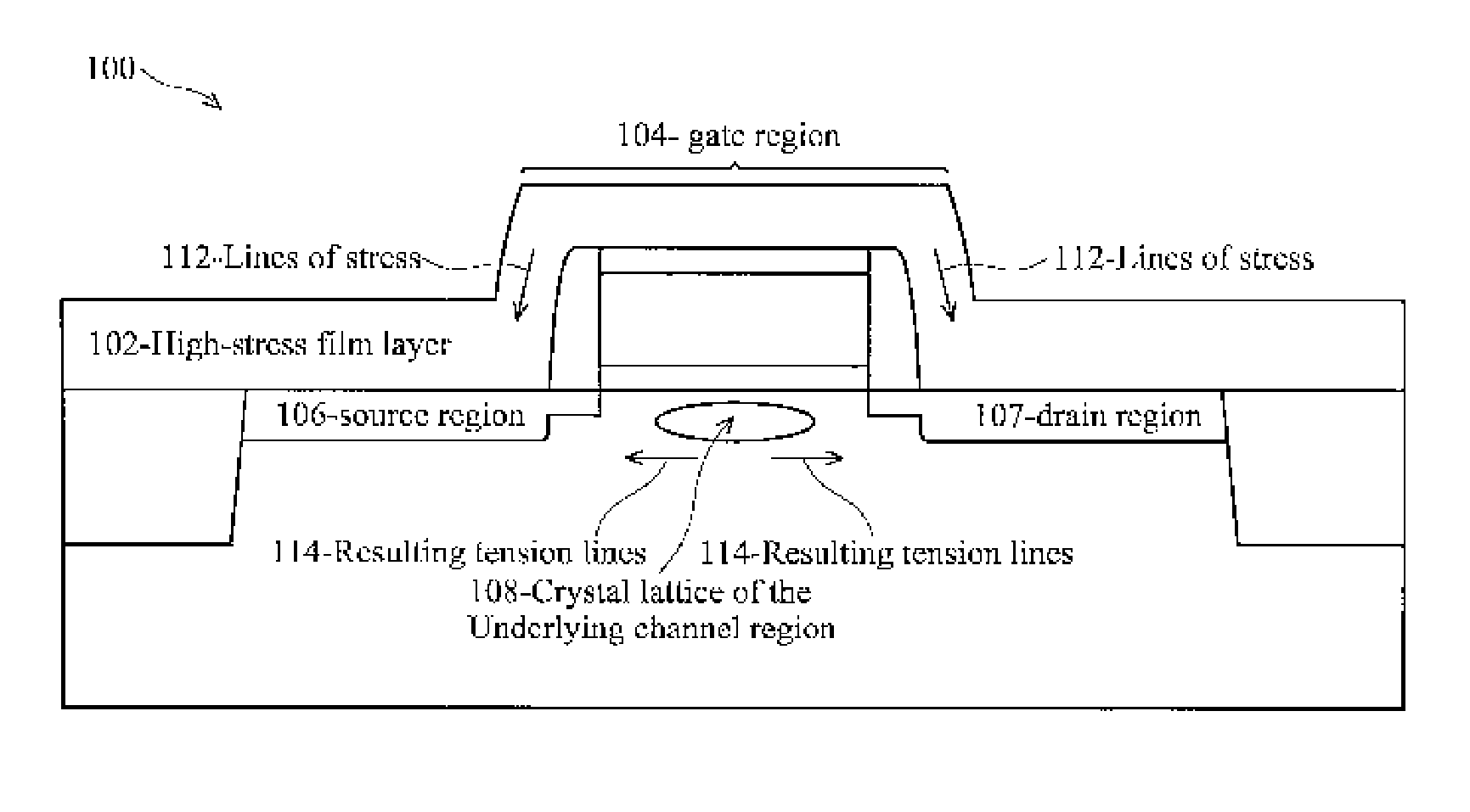
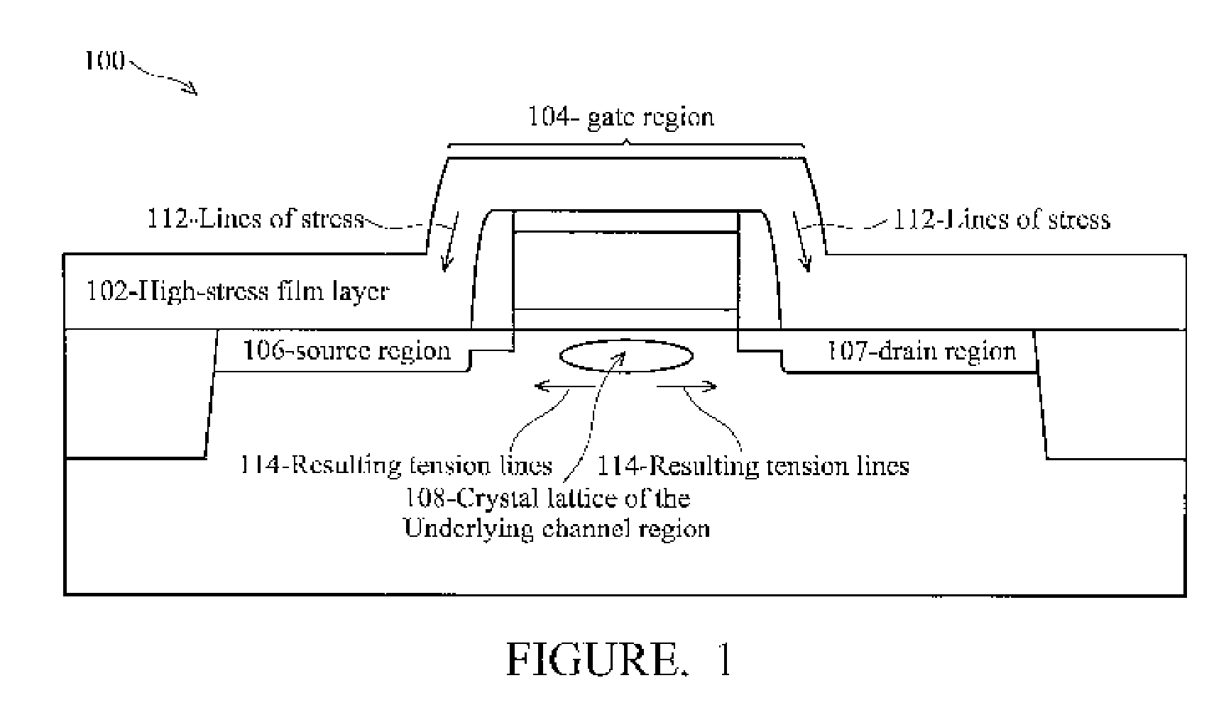
[0014]FIG. 1 is a cross-sectional diagram of a MOSFET transistor 100 in which a high-stress film layer 102 has been overlaid on the gate 104 and source / drain regions 106, 107 in order to impart a strain on the crystal lattice of the underlying channel region 108 of the transistor 100. Lines of stress 112 are drawn to illustrate the stresses built into the interface between the high-stress film layer 102, and the resulting tension lines 114 illustrate that a strain is imparted on the channel region 108 because of the pulling outward by the high-stress film 102 at the interface between the layers. According to Hooke's Law, stress is directly proportional to strain up to some proportionality constant. The above is a very general description of the elements of the MOSFET device 100. A number of the elements shown in this figure but not here described will be described in later figures as the process for forming the strain-inducing layer 102 and the higher carrier mobility MOSFET 100 is ...


PUM


Abstract

Described are methods of manufacturing a strain-inducing layer in semiconductor devices and structures formed to have such strain-inducing layers. Circuit elements are formed on a semiconductor substrate with conductive channel regions within the semiconductor substrate. Metal silicide contacts are formed on the semiconductor substrate and some are electrically connected to the channel regions. A strain-inducing layer can then be formed over the metal silicide contacts. Further, the strain-inducing layer is then treated with thermal processing, photo-thermal processing, or electron irradiation processing thereby increasing the stress of the strain-inducing layer and induce strain upon the crystal lattice structure in the conductive channel regions within the semiconductor substrate.

Description

BACKGROUND OF THE INVENTION [0001] Semiconductor devices operate by moving free, charged particles through a crystalline lattice structure. Ideally, these moving charged particles would pass through the crystalline lattice of a semiconductor without any collision or other atomic interaction with the lattice, as those interactions will inevitably impede the particles' progress. Accordingly, a material's resistivity (i.e., the material's resistance to the movement of charged particles through a material) will increase with greater particle interaction with the lattice. It is known that a regular crystalline lattice will interact more with free particles in it, and therefore will have a higher resistivity than an irregular crystalline lattice, such as one that is currently under a strain from adjacent materials. Conversely, a strained crystalline lattice will provide a higher charged particle mobility, as demonstrated in a study by Scott E. Thompson et al., A 90-nm Logic Technology Fea...

Claims


Application Information

Patent Timeline
IPC IPC(8): H01L29/94H01L21/3205
CPCH01L21/3105H01L21/76829H01L29/665H01L29/7843H01L29/7833
Inventor WU, ZHEN-CHENGHUANG, YU-LIENLU, YUNG-CHENG
Owner TAIWAN SEMICON MFG CO LTD
Why Eureka
Try Eureka