Method of forming a gate insulator in group III-V nitride semiconductor devices

a technology of nitride semiconductor devices and gate insulators, which is applied in the direction of semiconductor devices, basic electric elements, electrical equipment, etc., can solve the problems of limiting device performance, dielectric materials subject to undesirable thermal degradation, and premature breakdown of dielectric layers

Active Publication Date: 2006-06-08
TEKCORE CO LTD
View PDF1 Cites 26 Cited by
  • Summary
  • Abstract
  • Description
  • Claims
  • Application Information

AI Technical Summary

Problems solved by technology

However, a disadvantage of SiO2 or Si3N4 is its relatively low dielectric constant (about 3.9 for SiO2, and about 7.5 for Si3N4), which can cause a premature breakdown of the dielectric layer when the field effect transistor is operated at a high power voltage.
However, these dielectric materials are subject to undesirable thermal degradation due to a high interface state density of 1012 cm−2-eV−1.
This reflects a high crystal defect density, which seriously limits the device performance.

Method used


Image

  • Method of forming a gate insulator in group III-V nitride semiconductor devices
  • Method of forming a gate insulator in group III-V nitride semiconductor devices
  • Method of forming a gate insulator in group III-V nitride semiconductor devices

Examples


Embodiment Construction

)

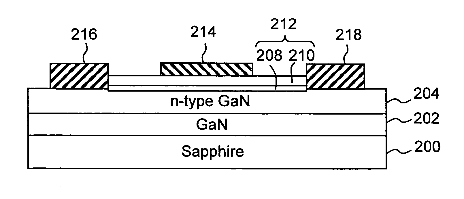
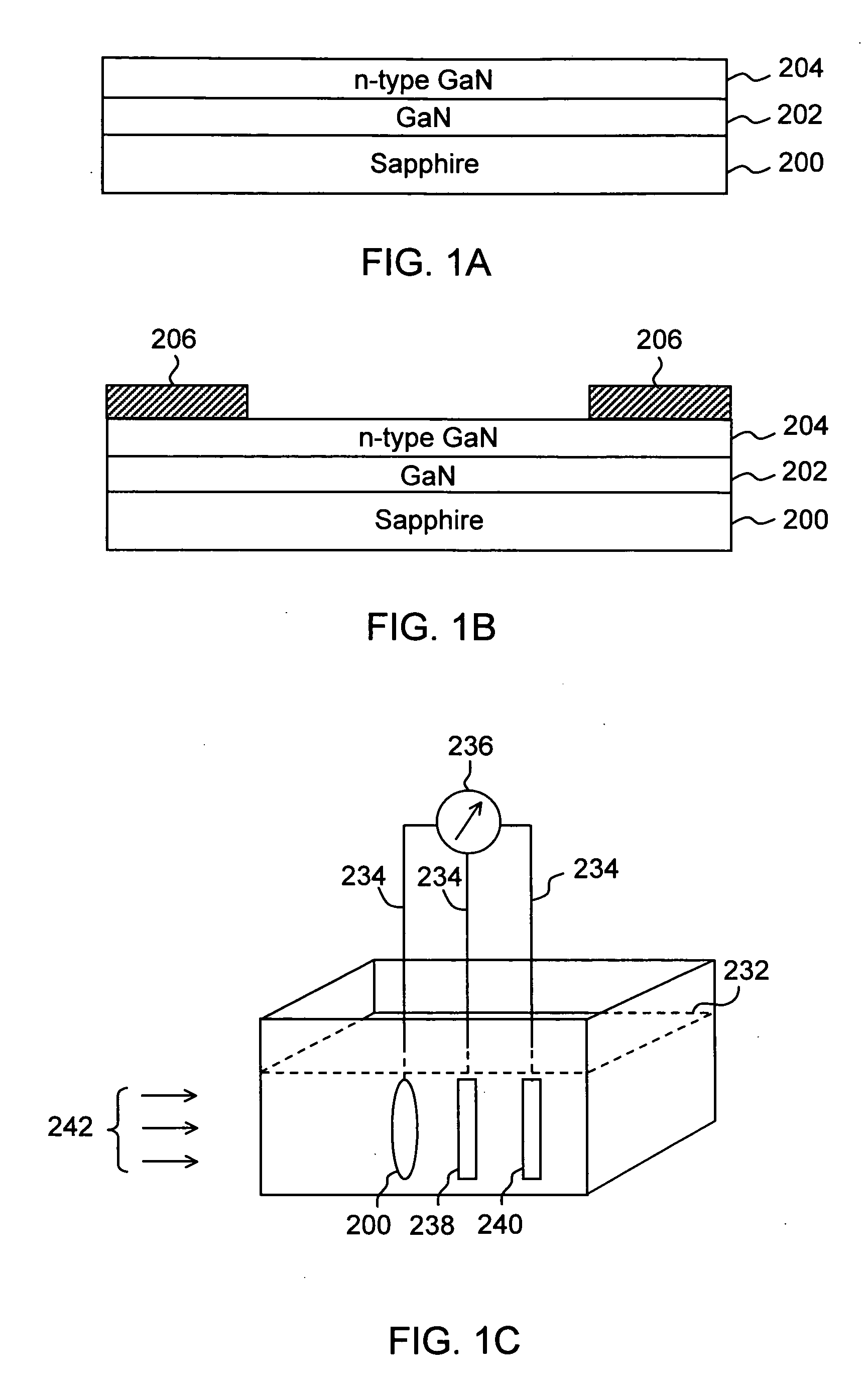
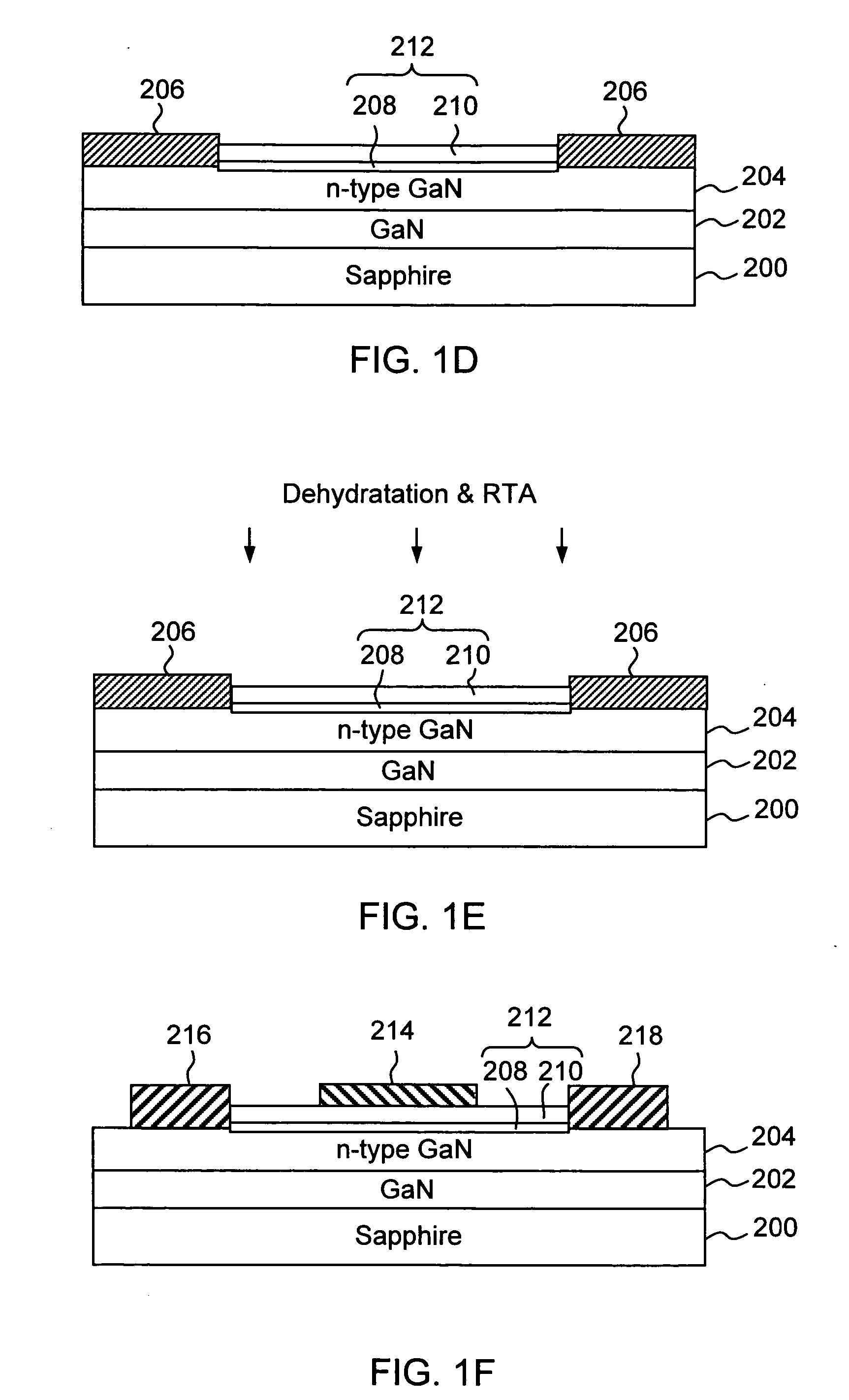
[0018] The present application describes a method of forming a gate insulator made of an oxide compound in the manufacture of a semiconductor device. In the embodiments herein, gallium oxide is described as a particular instance of the oxide compound since gallium oxide can be advantageously used as gate insulator for GaN-based semiconductor transistors, one type of III-V nitride semiconductor device developed in electronic and optoelectronic applications. However, the processing steps described herein are generally intended to be applicable for forming oxide compounds from any group III-V nitride semiconductor elements.

[0019] In the description hereafter, a group III-V nitride semiconductor element means GaN, InGaN, AlGaN, InAlGaN or the like.

[0020]FIG. 1A˜1F are schematic views describing a method of forming a group III-V nitride semiconductor device according to an embodiment of the invention. FIG. 1A illustrates an intermediate starting stage in which a buffer layer 202 and a...


PUM

PropertyMeasurementUnit
wavelengthaaaaaaaaaa
temperatureaaaaaaaaaa

Abstract

A method of forming a gate insulator in the manufacture of a semiconductor device comprises conducting a photo-assisted electrochemical process to form a gate-insulating layer on a gallium nitride layer of the semiconductor device, wherein the gate-insulating layer includes gallium oxynitride and gallium oxide, and performing a rapid thermal annealing process. The photo-assisted electrochemical process uses an electrolyte bath including buffered CH3COOH at a pH between about 5.5 and 7.5. The rapid thermal annealing process is conducted in O2 environment at a temperature between about 500° C. and 800° C.

Description

FIELD OF THE INVENTION [0001] The present invention generally relates to the manufacture of semiconductor devices, and more specifically to a method of forming a gate insulator in semiconductor devices and, particularly, group III-V nitride semiconductor devices. DESCRIPTION OF THE RELATED ART [0002] Electronic devices based on group III-V nitride compound semiconductors, and particularly gallium nitride (GaN) semiconductors, have been subject to intensive researches and developments in the field of electronic industry. Principal characteristics of GaN semiconductors include high electron mobility and saturation velocity (about 2.5×107 cm / s), and high breakdown electric field (about 5×10⁶V / cm), which make the GaN semiconductor particularly advantageous in high-power and high-temperature applications. [0003] In a GaN-based semiconductor device, the GaN semiconductor layers are conventionally grown over a substrate. To ensure good performances of the semiconductor device, it is known ...

Claims


Application Information

Patent Timeline
Patent Type & Authority Applications(United States)
IPC IPC(8): H01L21/84H01L21/20
CPCH01L21/02241H01L21/02258H01L21/02337H01L21/3143H01L21/31679H01L29/78681
Inventor PENG, LUNG-HANWU, HAN-MINGLIN, JING-YI
Owner TEKCORE CO LTD
Why Eureka
Try Eureka