Manufacturing method of vertical structure light emitting diode chip

A technology of light-emitting diodes and chips, which is applied in the direction of electrical components, circuits, semiconductor devices, etc., and can solve the problems of epitaxial wafer damage and low yield rate

Active Publication Date: 2018-11-23
山西中科潞安紫外光电科技有限公司
View PDF6 Cites 5 Cited by
  • Summary
  • Abstract
  • Description
  • Claims
  • Application Information

AI Technical Summary

Problems solved by technology

Generally, vertical structure LEDs are realized by laser lift-off, but it will cause damage to the epitaxial wafer, and the yield rate is low. Therefore, it is of great significance to develop new high-efficiency and low-loss vertical structure LED generation technologies.

Method used


Image

  • Manufacturing method of vertical structure light emitting diode chip
  • Manufacturing method of vertical structure light emitting diode chip

Examples


Embodiment Construction

[0030] In order to make the object, technical solution and advantages of the present invention clearer, the present invention will be described in further detail below in conjunction with specific embodiments and with reference to the accompanying drawings.

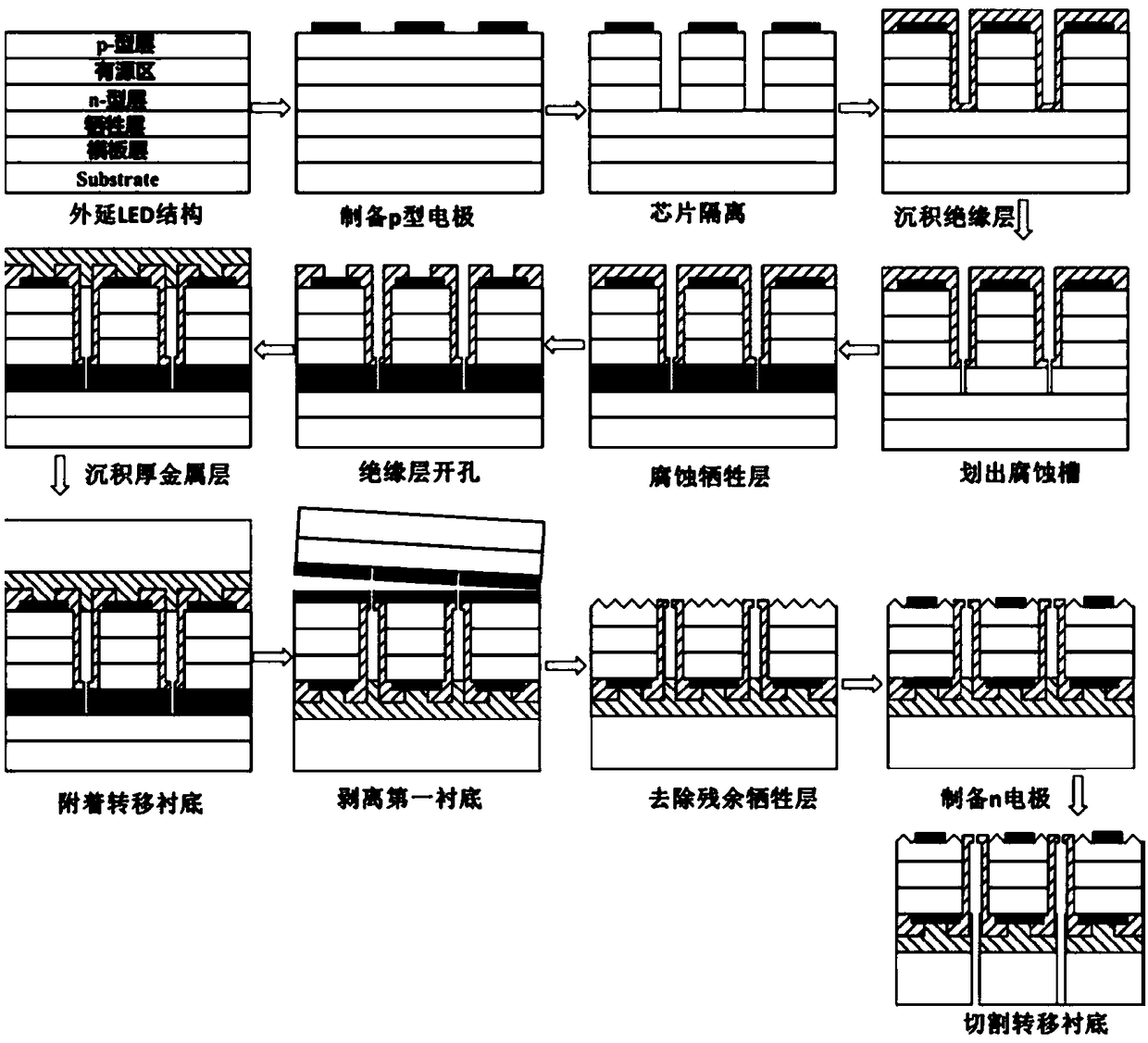
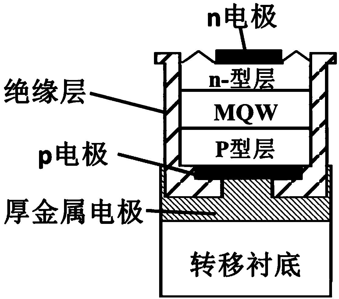
[0031] Vertical structure LED chip preparation method of the present invention, such as figure 1 As shown, it mainly includes the following steps:

[0032] Step 1. Epitaxial LED structure: On the first substrate, there are epitaxial template layer, sacrificial layer, n-type layer, active region and p-type layer sequentially from the substrate upward.

[0033] When selecting the first substrate, it should be considered that the crystal structure of the substrate material and the epitaxial material is the same or similar, the thermal expansion coefficient should match, and the substrate material should have good chemical stability. It should not be decomposed and corroded in the temperature and atmosphere of epitaxial growt...


PUM

PropertyMeasurementUnit
thicknessaaaaaaaaaa
emission peakaaaaaaaaaa

Abstract

The invention provides a preparing method of a vertical structure light-emitting diode (LED) chip. The preparing method corrodes a sacrificial layer in an epitaxial layer of an LED into a porous structure mainly through an electrochemical or photoelectrochemical etching or photo-assisted electrochemical etching method. The bonding strength between the upper and lower epitaxial layers of the sacrificial layer becomes quite weak, and the upper and lower epitaxial layers of the sacrificial layer can be easily peeled off. Compared with a vertical structure LED prepared by a laser lift-off method,the preparing method can solve the problem that the quality of an epitaxial layer material becomes poor due to laser ablation, and the yield is low.

Description

technical field [0001] The invention relates to the field of semiconductors, in particular to a method for manufacturing a vertical light emitting diode (LED) chip. Background technique [0002] LEDs based on III-nitrides have the characteristics of small size, high photoelectric conversion efficiency, long service life, fast response speed, and good shock and impact resistance. They have huge applications in lighting, display, optical communication, medical care, agriculture and other fields. space. In particular, LEDs in the ultraviolet band, compared with traditional ultraviolet light sources, are non-toxic and have continuously adjustable wavelengths, making them widely used in fields such as sterilization, air and water purification, medical beauty, polymer curing, biochemical detection, and non-line-of-sight communication. It has broad application prospects. [0003] At present, the most easily realized LED chip structure on a sapphire substrate is a lateral structur...

Claims


Application Information

Patent Timeline
Patent Type & Authority Applications(China)
IPC IPC(8): H01L33/00H01L33/62H01L33/64
CPCH01L33/005H01L33/62H01L33/64
Inventor 闫建昌张亮郭亚楠吴清清王军喜
Owner 山西中科潞安紫外光电科技有限公司
Why Eureka
Try Eureka