Method for manufacturing display device

a display device and manufacturing method technology, applied in semiconductor devices, liquid surface applicators, coatings, etc., can solve the problems of increasing manufacturing costs eventually, and achieve the effects of reducing costs, good controllability, and minimal material loss

Inactive Publication Date: 2006-06-08
SEMICON ENERGY LAB CO LTD
View PDF7 Cites 59 Cited by
  • Summary
  • Abstract
  • Description
  • Claims
  • Application Information

AI Technical Summary

Benefits of technology

[0018] According to the present invention, a desired pattern can be formed with good controllability, and cost can be reduced with minimal loss of materials, making it possible to manufacture a high-performance and highly reliable display device at good yield.

Problems solved by technology

Increasing the number of processes for photolithography increases the manufacturing cost eventually.

Method used


Image

  • Method for manufacturing display device
  • Method for manufacturing display device
  • Method for manufacturing display device

Examples


embodiment mode 1

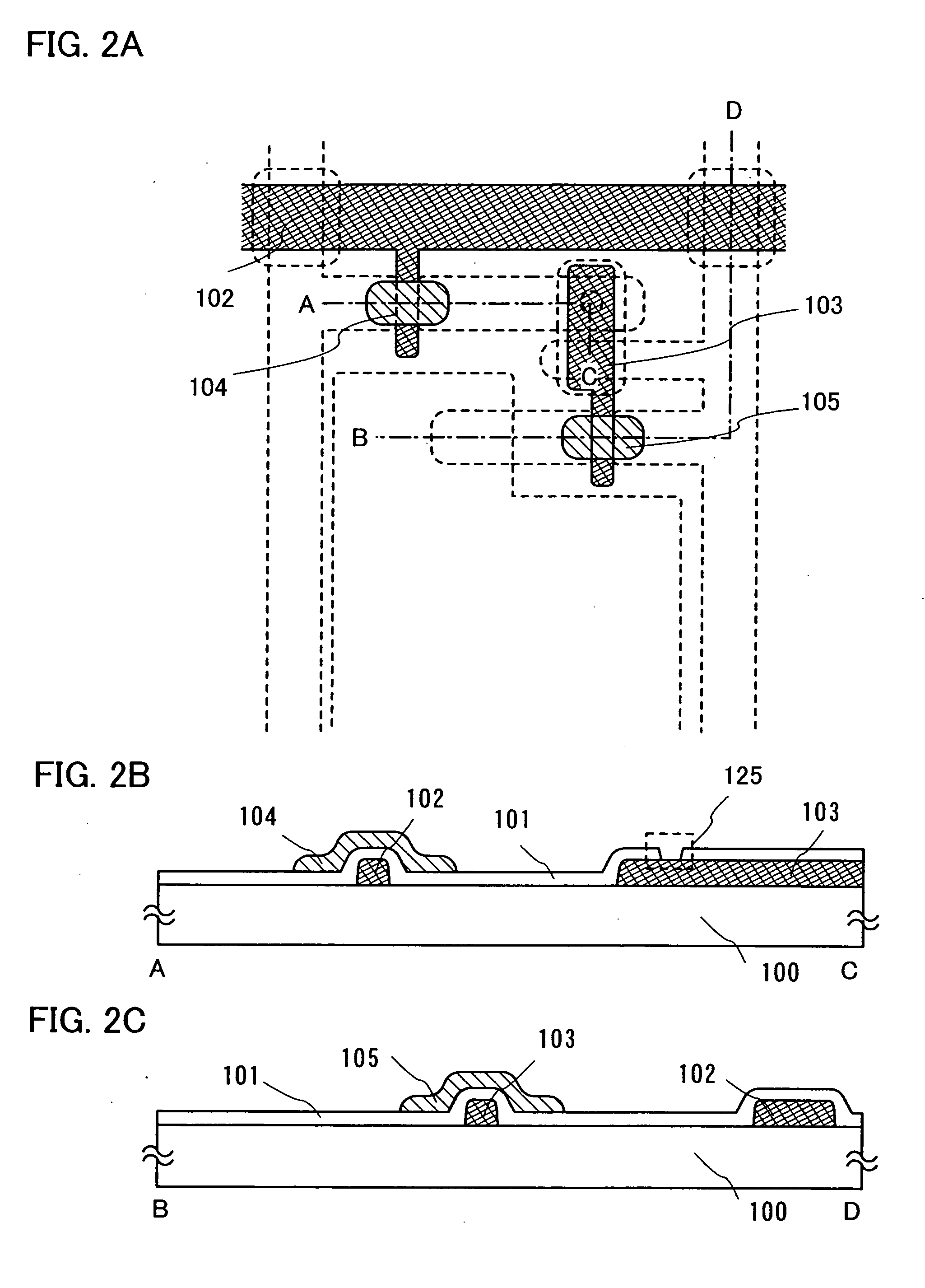
[0050]FIG. 25(A) is a top view showing a structure of a display panel according to the present invention. A pixel portion 2701 in which pixels 2702 are arranged in a matrix form, a scanning line side input terminal 2703 and a signal line side input terminal 2704 are formed over a substrate 2700 with an insulated surface. The number of pixels may be determined in accordance with various standards. The number of pixels for XGA may be 1,024×768×3 (RGB), and that for UXGA may be 1,600×1,200×3 (RGB). In the case of forming a display panel corresponding to a full-specification high-definition, the number of pixels may be 1,920×1,080×3 (RGB).

[0051] The pixels 2702 are arranged in a matrix form by intersecting scanning lines that extend from the scanning line side input terminal 2703 with signal lines that extend from the signal line side input terminal 2704. Each pixel 2702 includes a switching element and a pixel electrode connecting to the switching element. A TFT is a representative ex...

embodiment mode 2

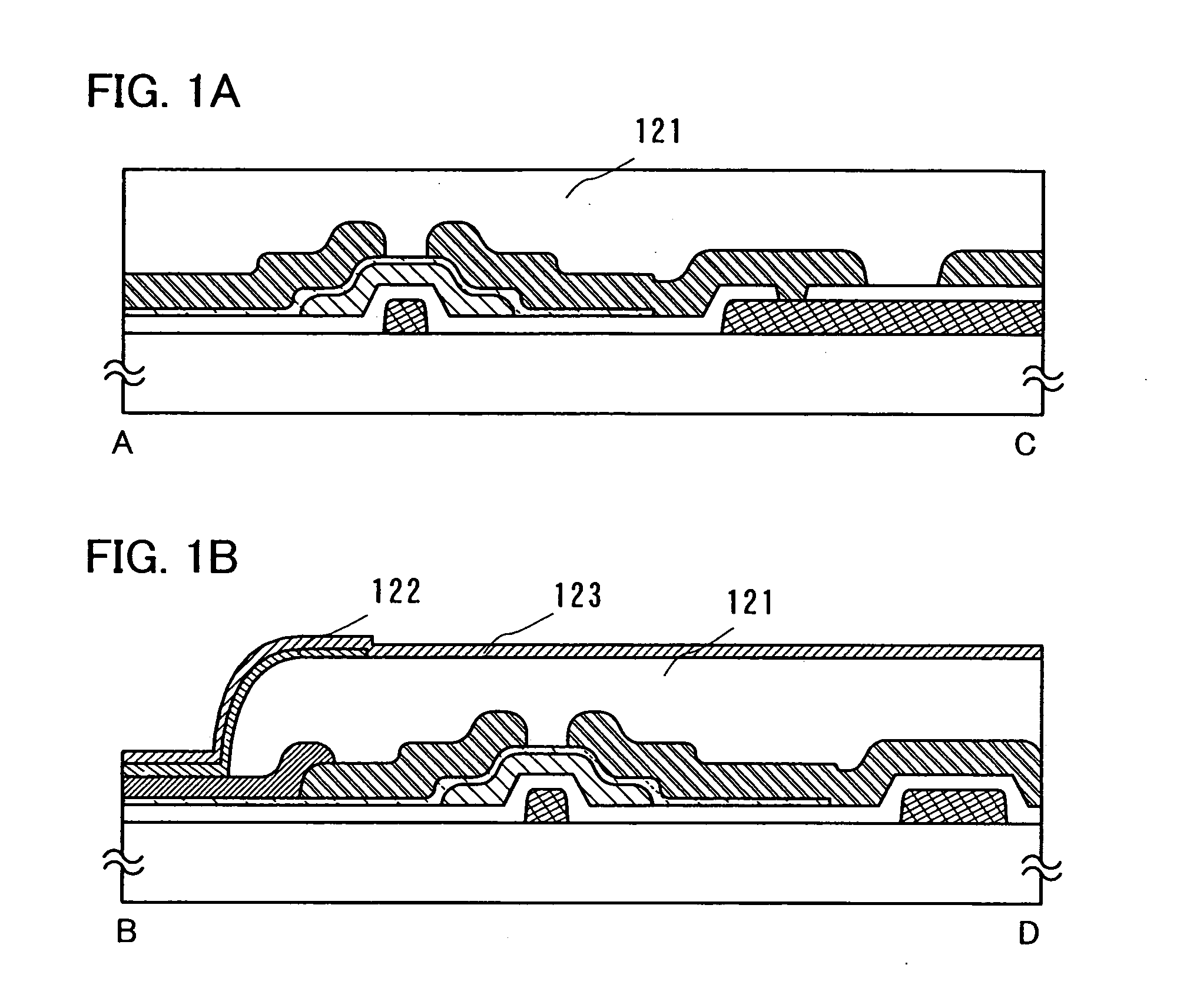
[0141] An embodiment mode of the present invention will be described using FIG. 8 to FIG. 11(B). Specifically, a method for manufacturing a display device having a coplanar type thin film transistor to which the present invention is applied will be described. FIG. 8 is a top view of a pixel portion of a display device. FIG. 9(A) to FIG. 10(C) are cross sectional views along a line E-F of FIG. 8 showing respective process of manufacturing the display device. FIG. 11(A) is also a top view of the display device. FIG. 11(B) is a cross sectional view along a line O-P (including a line U-W) of FIG. 11(A). Further, an example of a liquid crystal display device that uses a liquid crystal material as a display element is shown. Therefore, the same portions or portions having the same functions will not be repeatedly explained.

[0142] A gate electrode layer 254a, a gate electrode layer 254b, and a gate electrode layer 254c are formed over a substrate 250 having a light-transmitting property. ...

embodiment mode 3

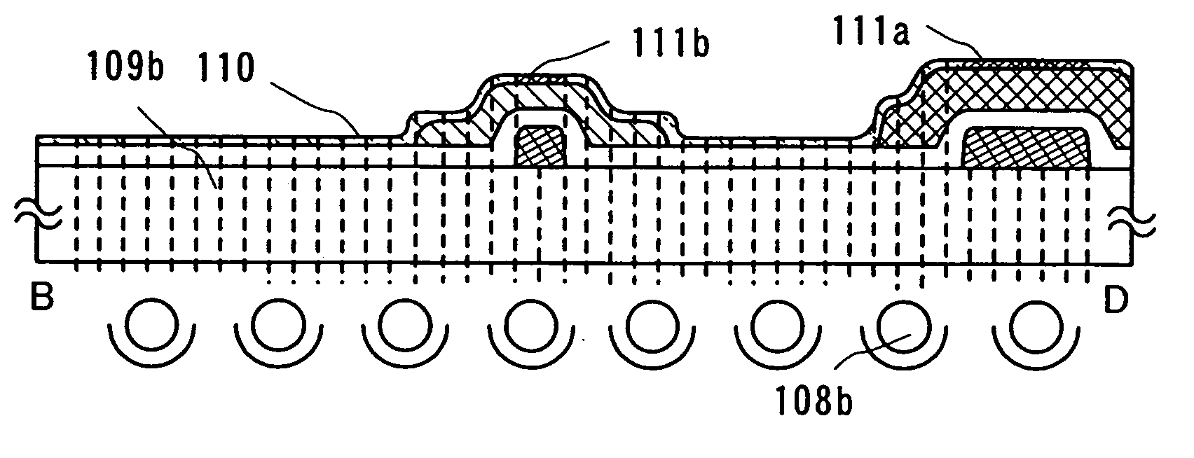
[0181] An embodiment mode according to the present invention will be described with reference to FIG. 12(A) to FIG. 17(B). In this embodiment mode, a display device is formed using a thin film transistor of inverted coplanar type as a thin film transistor. An example of a liquid crystal display device using a liquid crystal material as a display element is shown. Accordingly, the same part or a part having similar function will not be repeatedly explained. Each of FIG. 12(A) to FIG. 17(A) shows a top view of a display device, each of FIG. 12(B) to FIG. 17(B) shows a cross-sectional view taken along line G-H in FIG. 12(A) to FIG. 17(A).

[0182] Also in this embodiment mode, a light irradiation treatment is carried out through a substrate to modify the irradiated region to change the wettability thereof by using the photo activity of a photocatalytic substance.

[0183] A gate electrode layer 301 and a gate electrode layer 303, and a capacitor wiring layer 326 are formed on the substrate...


PUM


Abstract

The present invention, the quality of the surface of a substrate is improved and the wettability thereof is controlled by light irradiation from the reverse side with respect to the substrate having the conductive layer. A conductive material or an insulating material is adhered on the modified surface by discharging it (including jetting, etc.), or the like to form a conductive layer and an insulating layer. The processing efficiency by the light can be enhanced by function of the light absorption and energy radiation of the photocatalytic substance. Furthermore, the mask layer is formed selectively on the conductive layer and the wettability of the region on the conductive layer that is a non-irradiation region is also controlled.

Description

TECHNICAL FIELD [0001] The present invention relates to a method for manufacturing a display device. BACKGROUND ART [0002] A thin film transistor (hereinafter, also referred to as a TFT) and an electronic circuit using the TFT have been formed as follows: various kinds of thin films such as a semiconductor, an insulator, and a conductor are laminated over a substrate, and the thin films are processed into a predetermined pattern appropriately by a photolithography technique. The photolithography technique is a technique for transferring a pattern such as a circuit which is formed of a light-shielding material over a flat transparent plate that is referred to as a photomask, over a substrate by using light. The technique has been widely used in a process of manufacturing a semiconductor integrated circuit and the like. [0003] In the conventional manufacturing process using the photolithography technique, many processes such as light-exposing, developing, baking, and separating are re...

Claims


Application Information

Patent Timeline
Patent Type & Authority Applications(United States)
IPC IPC(8): H01L21/31B05D5/12H01L21/469
CPCH01L21/288H01L21/76838H01L27/1214H01L27/3244H01L51/0004H01L27/1288H10K59/12H10K71/13
Inventor FUJII, GEN
Owner SEMICON ENERGY LAB CO LTD
Why Eureka
Try Eureka