Large-sized light-emitting diodes with improved light extraction efficiency

a light-emitting diode and large-scale technology, applied in the field of semi-conductor light-emitting devices, can solve the problems of reducing the internal quantum efficiency of the led chip, and increasing the temperature of the chip, so as to improve the light extraction efficiency of the light-emitting diode chip, reduce the length of the optical path, and increase sidewall areas

Inactive Publication Date: 2006-06-15
ELITE OPTOELECTRONICS
View PDF5 Cites 20 Cited by
  • Summary
  • Abstract
  • Description
  • Claims
  • Application Information

AI Technical Summary

Benefits of technology

[0010] It is one objective of the present invention to provide a light-emitting device employing a design of an array of window openings to create a larger sidewall area within an emitting area thereof to enhance light extraction from this device.
[0011] It is another objective of the present invention to provide a large-sized light-emitting diode chip with an array of window openings to efficiently extracting photons trapped inside the large-sized light-emitting diode chip.
[0013] The window openings within the emitting area of the light-emitting diode chip increase sidewall areas within the emitting area, and hence reduce the length of optical path before photons can reach the sides of the light-emitting diode chip. The photons traveling inside the light-emitting diode chip can easily escape from the sidewalls of these window openings before they are absorbed. The light extraction efficiency of the light-emitting diode chip is improved.

Problems solved by technology

Unfortunately, when a LED chip is driven with high current density, the chip is heated and the temperature of this chip increases.
High temperature can reduce the radiative recombination rate to decrease the internal quantum efficiency of the LED chip and thus the performance is reduced as well.
However it has been shown that the external quantum efficiencies of LEDs go down when the sizes of LEDs are increased.
One of the constraints of sizing up a LED chip is the inability to effectively spread the electric current uniformly over the entire LED.
Because of current crowding effect, the electric current could concentrate at certain regions on a LED chip to induce local heating and to cause premature degradation of the device.
The current crowding effect can degrade the performance more on large-sized LED chips since the distribution of electric current over large-sized LEDs is much more difficult.
Another constraint is the absorption loss of photons within the semiconductor thin film.
The loss of photons due to the absorption drastically reduces the performance of large-sized LEDs.

Method used


Image

  • Large-sized light-emitting diodes with improved light extraction efficiency
  • Large-sized light-emitting diodes with improved light extraction efficiency
  • Large-sized light-emitting diodes with improved light extraction efficiency

Examples


Embodiment Construction

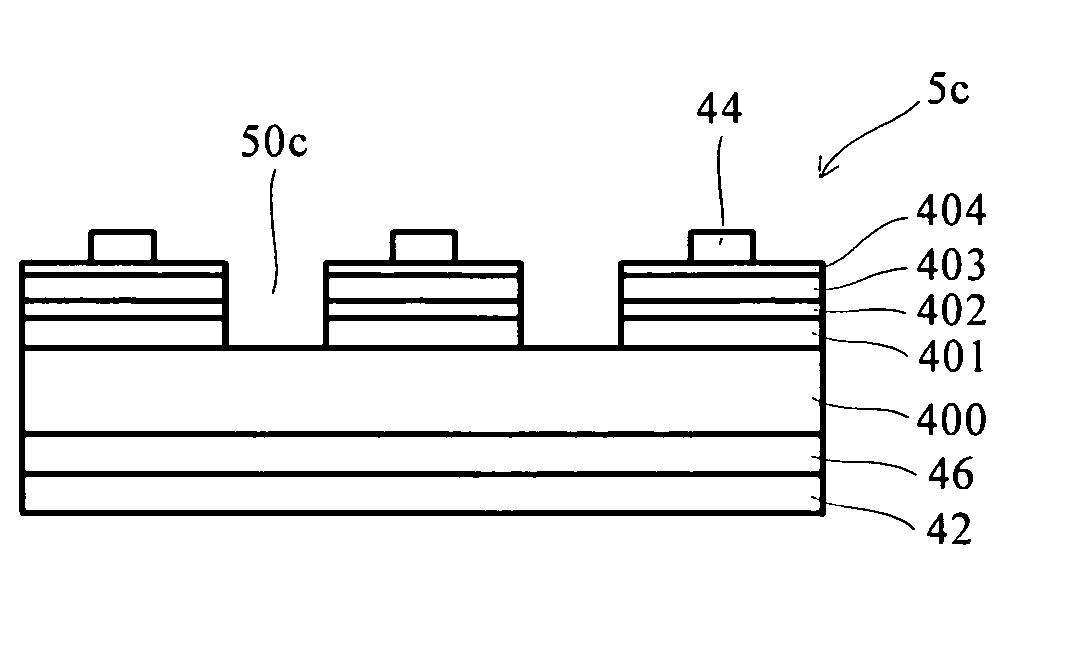
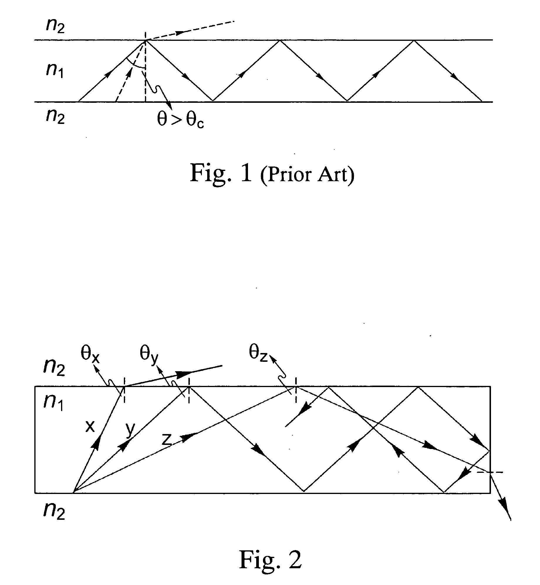
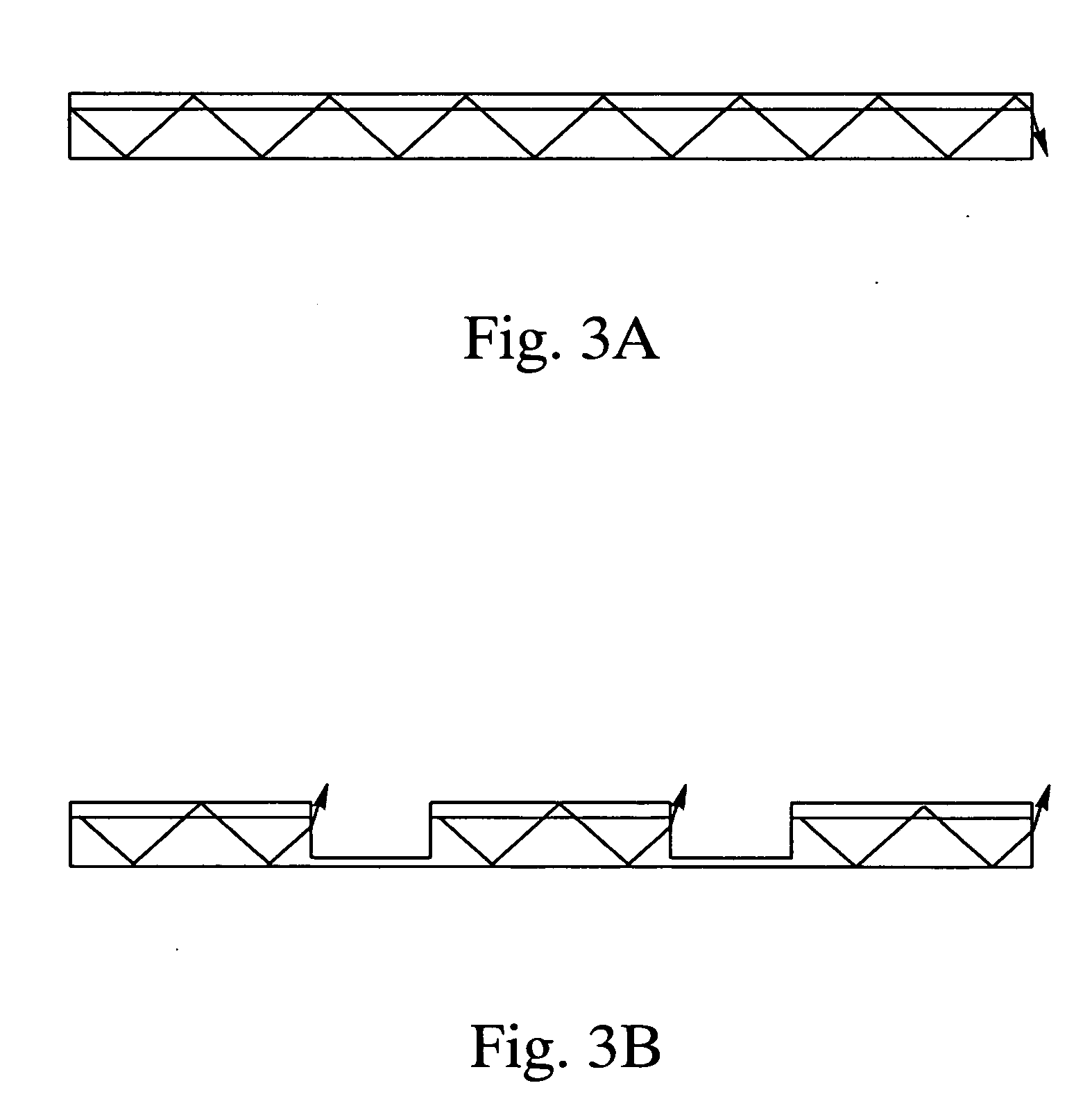
[0030] The present invention is a light-emitting device with an array of window openings to enhance the light extraction efficiency from this device. This array of window openings is employed to create a much larger sidewall area to enhance the light extraction from the sidewall of these openings. With this array of window openings, photons trapped due to the total internal reflection can propagate within the device and be extracted from the sidewall of these openings. It is of great importance for large-sized LEDs to extract photons employing this array of window openings because of the huge loss of photons caused by absorption. These openings are created by etching deep into the epitaxial layer or may be even down to the substrate. A variation of designs can be applied to the array of window openings. The window openings can be etched very rough to enhance the light emission from the sidewall; or reflected mirrors can be fabricated in the windows to redirect photons escaping from ...


PUM


Abstract

A light-emitting device with an array of window openings to enhance the light extraction efficiency from this device is provided. This array of window openings is employed to create a much larger sidewall area to enhance the light extraction from the sidewalls of these openings. With this array of window openings, photons trapped due to the total internal reflection can propagate within the device and be extracted from the sidewalls of these openings. A variation of designs can be applied to the array of window openings. Even the shape of these openings can be designed such that the area of the sidewalls is increased. Large-sized light-emitting diodes can improve the light extraction efficiency by employing the array of window openings.

Description

BACKGROUND OF THE INVENTION [0001] 1. Field of the Invention [0002] The present invention relates to semiconductor light-emitting devices, and more particularly, to the improvement of the light extraction from such devices. [0003] 2. Description of the Related Art [0004] A light emitting diode (LED) is a forward-biased p-n junction generating photons by spontaneous electron-hole pair recombination. The first practical p-n junction LED was reported by Nathan in 1962. After decades of development, LED technology has been greatly advanced by improved materials qualities, new material systems, and novel structures. Today, for visible long-wavelength LEDs, i.e. red, yellow, orange, and amber LEDs, the emission efficiencies are superior to incandescent lamps. Meanwhile, very efficient green and blue LEDs have also been successfully achieved since the epitaxy technology of III-V nitride materials has been rapidly developed for last several years. The III-V nitride material system is a grou...

Claims


Application Information

Patent Timeline
Patent Type & Authority Applications(United States)
IPC IPC(8): H01L33/00H01L33/08H01L33/20H01L33/38H01L33/46
CPCH01L33/08H01L33/20H01L33/38H01L33/46
Inventor LI, YUN LISO, WILLIAN WILSONLIU, HENG
Owner ELITE OPTOELECTRONICS
Why Eureka
Try Eureka