

Solid-state imaging element, solid-state imaging device, and method for fabricating the same
a solid-state imaging and element technology, applied in the field can solve the problems of color separation becoming more difficult, obstacle to miniaturization of solid-state imaging elements, and the inability to enhance light condensation beyond certain limits, and achieve the effect of efficient light condensation and low loss
- Summary
- Abstract
- Description
- Claims
- Application Information
AI Technical Summary
Benefits of technology
Problems solved by technology
Method used
Image

Examples
first embodiment
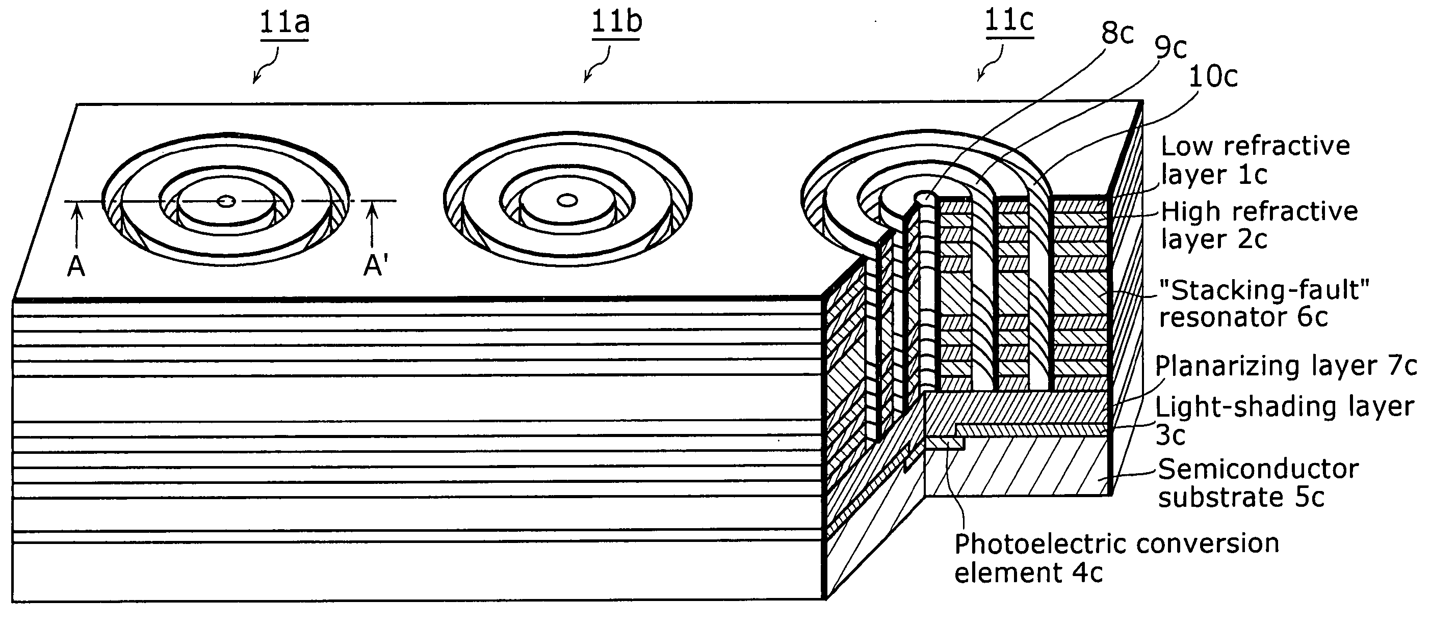
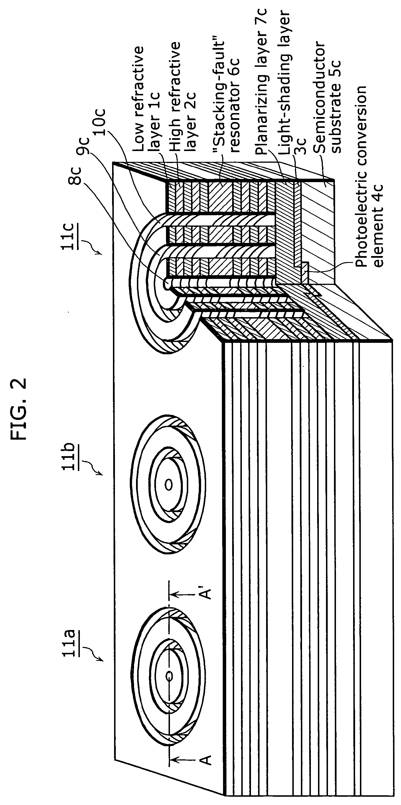
[0037]FIG. 2 is an external view of solid-state imaging elements 11a, 11b and 11c in the present embodiment. For example, the structure of the solid-state imaging element 11c is as follows: A photoelectric conversion element 4c for converting incident light into signal charge is provided on the surface of a semiconductor substrate 5c; a light-shading layer 3c for cutting off the incident light from the side is provided along the side of the window upon the photoelectric conversion element 4c; a planarizing layer 7c is provided over the light-shading layer 3c and the photoelectric conversion element 4c; and a photonic crystal having a multi-layer structure to be described later, as an optical element, is provided on the planarizing layer 7. As shown in FIG. 2, the photonic crystal of the solid-state imaging element 11c includes a central cavity 8c and two doughnut-shaped longitudinal cavities 9c and 10c around the central cavity 8c. In other words, five concentric circles can be seen...
second embodiment
[0055] Next, a solid-state imaging element in the second embodiment will be explained. This solid-state imaging element is different from that in the first embodiment in the structure of a photonic crystal and the method for fabricating it.
[0056]FIG. 10 is an external view of solid-state imaging elements 12a, 12b and 12c in the present embodiment. For example, the structure of the solid-state imaging element 12c is as follows: a photoelectric conversion element 4c for converting incident light into signal charge is provided on the surface of a semiconductor substrate 5c; a light-shading layer 3c for cutting off the incident light from the side is provided along the side of the window upon the photoelectric conversion element 4c; and a photonic crystal to be described later, as an optical element, is provided on the light-shading layer 3c and the photoelectric conversion element 4c so that the center of the concentric pattern thereof is aligned with the center of the photoelectric c...
PUM
 Abstract
Description
Claims
Application Information