Fast heating and cooling wafer handling assembly and method of manufacturing thereof

a wafer and assembly technology, applied in lighting and heating apparatus, muffle furnaces, furnaces, etc., can solve the problems of limited thermal budget, wafer defects, and limited thermal processing speed,

Inactive Publication Date: 2006-06-15
GENERAL ELECTRIC CO
View PDF5 Cites 277 Cited by
  • Summary
  • Abstract
  • Description
  • Claims
  • Application Information

AI Technical Summary

Benefits of technology

[0010] The invention further relates to a method for treating at least a semiconductor wafer substrate in which the processing cycle comprises conduction heating for heating the wafer substrate to the desired proce

Problems solved by technology

The thermal budget is limited by adverse effects on the wafer; too hot, too long, or any excursion from a prescribed time-temperature recipe can cause defects in the wafer.
However, the need to wait for conditions in the furnace to reach steady state for uniform results typically requires long processing times, which may violate limitations imposed by the thermal budget or the process recipe.
However, due to temperature uniformity requirements, rapid thermal processing is typically limited to single-wafer processing.
However, these systems are complex

Method used


Image

  • Fast heating and cooling wafer handling assembly and method of manufacturing thereof
  • Fast heating and cooling wafer handling assembly and method of manufacturing thereof
  • Fast heating and cooling wafer handling assembly and method of manufacturing thereof

Examples


example 1

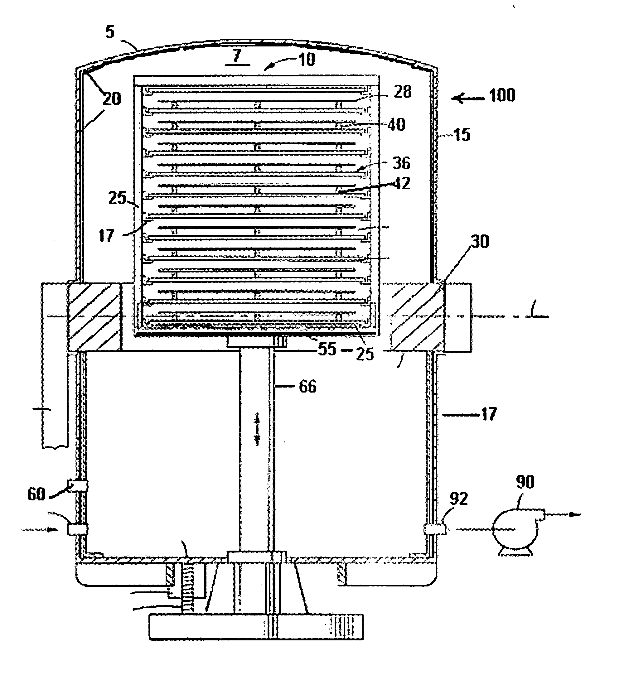
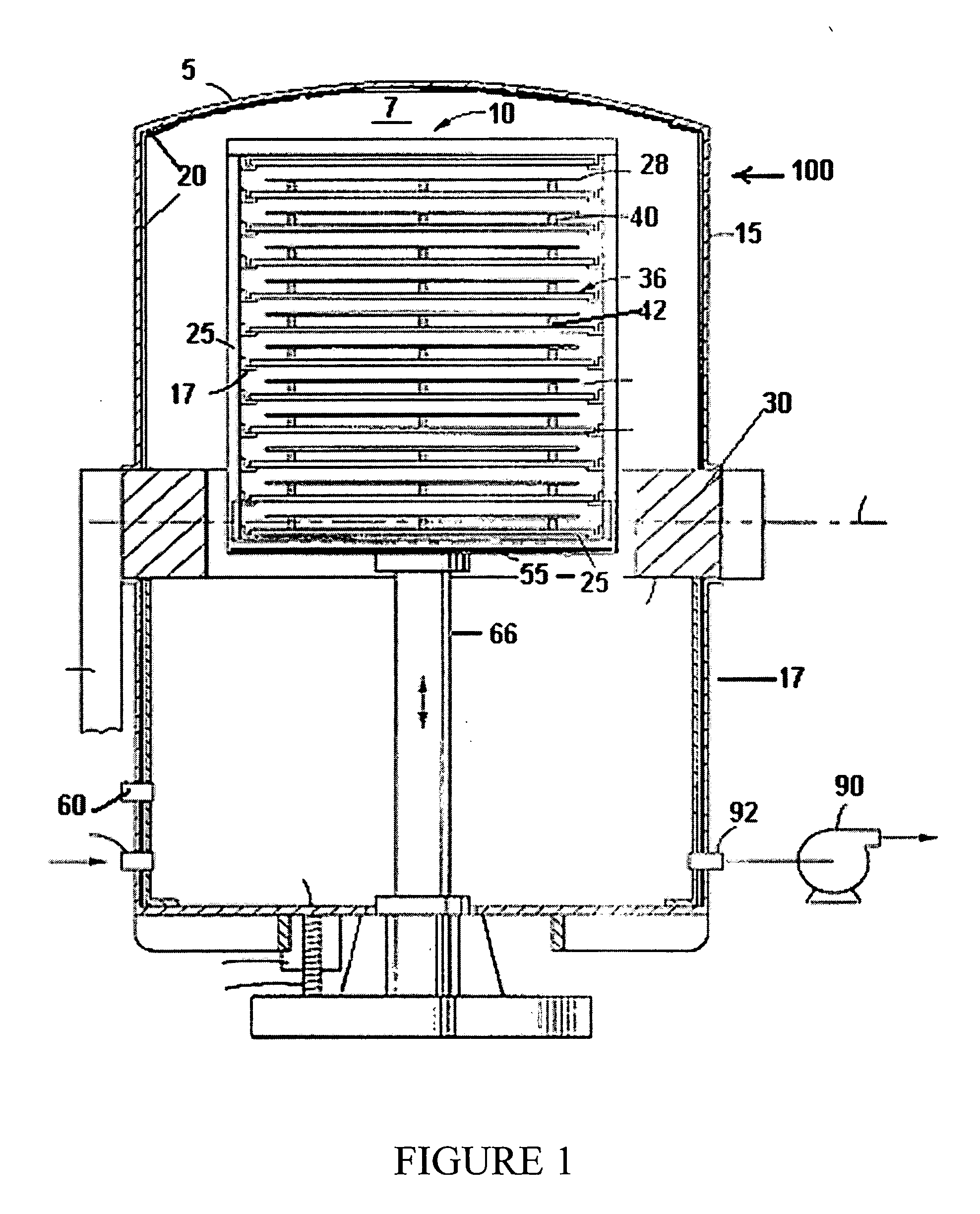
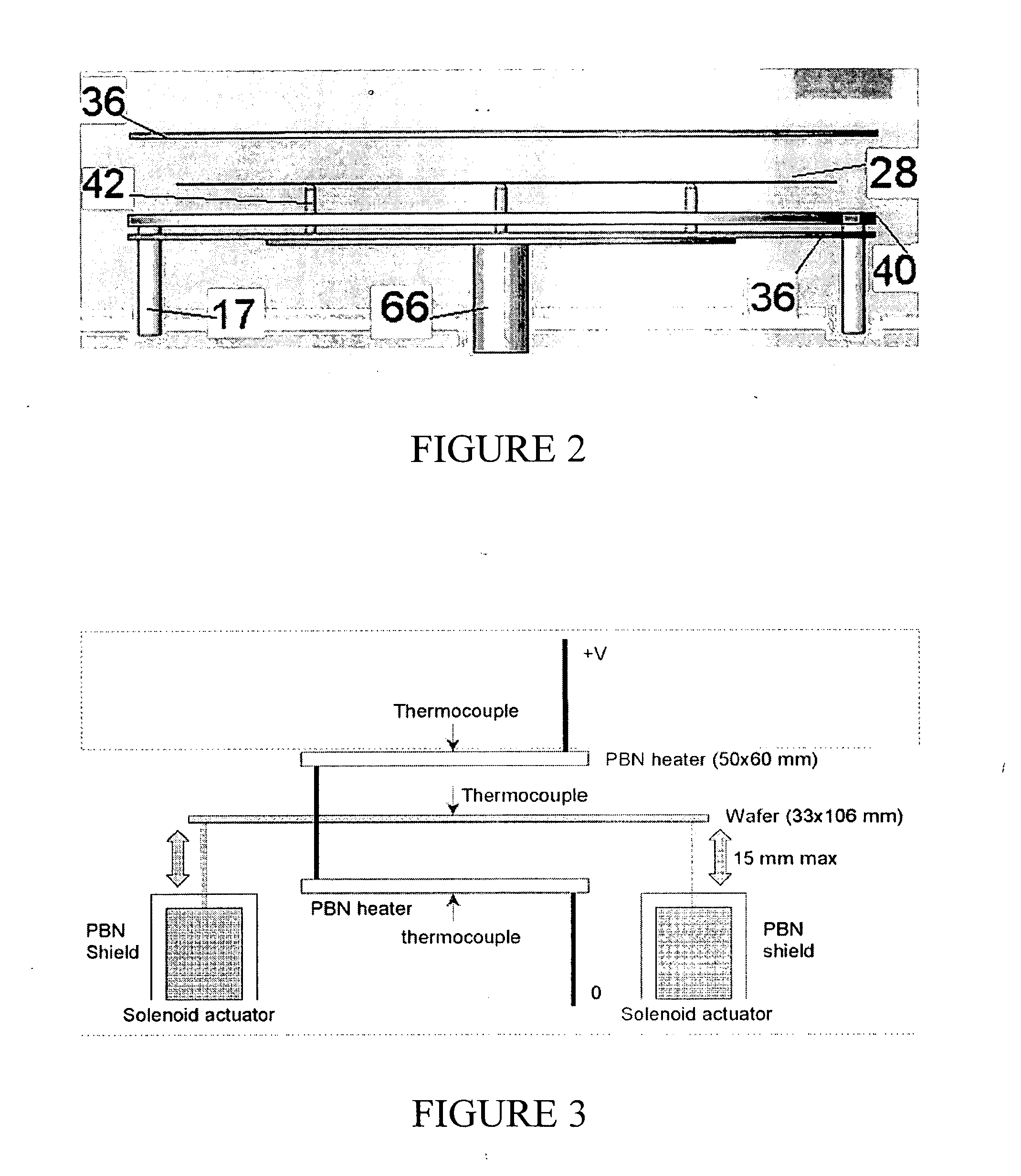
[0069] A series of tests are conducted on a silicon wafer positioned in-between two heaters from General Electric Company sold under the trade name BORAELETRIC. A sketch of the set up is as illustrated in FIG. 3. The wafer is supported by three solenoid actuators, so that the wafer rested on the bottom heater when the solenoid arms are fully retracted. Simultaneously powering the solenoid actuators extends the solenoid arms, such that the wafer can be lifted from the bottom heater and positioned halfway in-between the two heaters. Fast-response wire thermocouples are used to measure temperature on the wafer surface at various points. The power input to the heaters is varied as a function of time. Time at which the solenoids are powered (wafer lift-off time) can also be adjusted.

[0070] For each test, the wafer is first heated at high power in a conduction mode for a period of time ranging from 5 to 30 seconds (“transition time”) to obtain the desired process temperature. At the tran...

example 2

[0072] A series of tests are conducted with a set-up including a wafer supported by three solenoid actuators. The wafer is located above a GE Boralectric heater such that the wafer rests on the heater when the solenoid arms are fully retracted. When the solenoid actuators are powered, they extend the solenoid arms such that the wafer is lifted above the heater.

example 3

[0073] A heat reflector is used in conjunction with the set up of Example 1. The results of the test show that the presence of a heat reflector effectively increases the heating rate and reduces the thermal budget of the process.

[0074] Representative data from Examples 1 and 2 tests are illustrated in FIG. 4. As shown, a suitable combination of time-dependent heater power input and wafer lift-off time allows a specified wafer temperature profile of fast thermal cycling processes, i.e. consisting of at least one fast heating period (conduction mode), one constant temperature portion (radiation mode), and an optional fast cooling period. The graph illustrates a suitable time-dependent combination of two heating modes, a conduction heating mode first for rapid heating (wafer heating rate >10° C. / s), followed by a radiation heating step for maintaining a constant temperature profile. In some of the tests, the wafer heating rate is >20° C. / s. Additionally, a suitable time-dependent comb...


PUM


Abstract

A thermal control device for wafer processing which comprises a) a platform for placement of an object of various sizes to be heated, b) at least a shaft extending substantially transverse to the platform; and c) a plurality of resistance heating elements patterned in a plurality of circuits defining at least one zone for independent controlled heating of objects of varying sizes on the platform.

Description

CROSS-REFERENCE TO RELATED APPLICATIONS [0001] This application claims the benefits of U.S. Provisional Patent Application Ser. No. 60 / 635636 filed Dec. 13, 2004, and U.S. Provisional Patent Application Ser. No. 60 / 650392 filed Feb. 4, 2005, which patent applications are fully incorporated herein by reference.FIELD OF THE INVENTION [0002] The invention relates generally to a wafer-handling assembly for use in the manufacture of semiconductors. BACKGROUND OF THE INVENTION [0003] Wafer handling assemblies are used in a number of system applications such as molecular beam epitaxy, space experiments, and substrate heaters for electron microscopy and in the growth of superconducting films, etc. A wafer-processing chamber or assembly is a device that heats objects, such as semiconductor wafers. In semiconductor wafer processing, fast heating and cooling cycles are often needed in steps such as annealing or degassing. These steps usually consist of any number of fast heating processes, som...

Claims


Application Information

Patent Timeline
IPC IPC(8): F27B5/14
CPCF27B5/04F27B17/0025H01L21/67109H01L21/67248H01L21/324H01L21/02
Inventor WINTENBERGER, ERICPRASAD, SRIDHAR R.MARINER, JOHNLU, ZHONG-HAO
Owner GENERAL ELECTRIC CO
Why Eureka
Try Eureka