Method for forming a titanium nitride layer and method for forming a lower electrode of a MIM capacitor using the titanium nitride layer

a technology of titanium nitride and capacitor, which is applied in the direction of coating, solid-state devices, chemical vapor deposition coating, etc., can solve the problems of deteriorating the characteristic of transistors, deficient constant capacitance, and crystalline silicon or polysilicon, so as to prevent diffusion of impurities, improve the effect of surface area and good quality

Inactive Publication Date: 2006-06-15
SAMSUNG ELECTRONICS CO LTD
View PDF11 Cites 17 Cited by
  • Summary
  • Abstract
  • Description
  • Claims
  • Application Information

AI Technical Summary

Benefits of technology

[0015] According to the embodiment of the present invention, the titanium nitride layer produced with the aforementioned method has a good quality and an increased surface area which makes it useful for forming the lower electrode of a MIM capacitor.
[0016] In another embodiment of the present invention, the RTP at a high temperature of about 600° C. to about 700° C., is preferably performed for a short period in order to prevent diffusion of impurities out of an impurity region of the transistor. For example, the RTP may be carried out for any short period, but preferably, for about 10 seconds to about 60 seconds.

Problems solved by technology

The single crystalline silicon or the polysilicon, however, shows a limitation in reducing the resistance of the capacitor electrodes due to its material characteristic.
This material characteristic limitation is manifested when a bias voltage is applied to the capacitor electrodes made of the single crystalline silicon or polysilicon resulting in a deficient constant capacitance due to a generation of a depletion region and an unstable voltage in the capacitor.
In turn, these impurities may diffuse out of the impurity region of the substrate and eventually deteriorate the characteristic of a transistor which may constitute a logic area of a device.
These impurities may deteriorate the characteristics of the titanium nitride layer due to an increase in its resistivity.
In addition, said impurities may react with a dielectric layer of the ensuing product capacitor, leading to an increase in leakage current.
However, this approach of forming a metal lower electrode with an increased surface area to secure a high capacitance has yet to be tried.

Method used


Image

  • Method for forming a titanium nitride layer and method for forming a lower electrode of a MIM capacitor using the titanium nitride layer
  • Method for forming a titanium nitride layer and method for forming a lower electrode of a MIM capacitor using the titanium nitride layer
  • Method for forming a titanium nitride layer and method for forming a lower electrode of a MIM capacitor using the titanium nitride layer

Examples


Embodiment Construction

[0027] Detailed references to the preferred embodiments of the present invention will now be made; examples of which are illustrated in the accompanying drawings. However, the present invention is not limited to the embodiments illustrated hereinafter, where the embodiments herein are introduced for understanding the scope and spirit of the present invention.

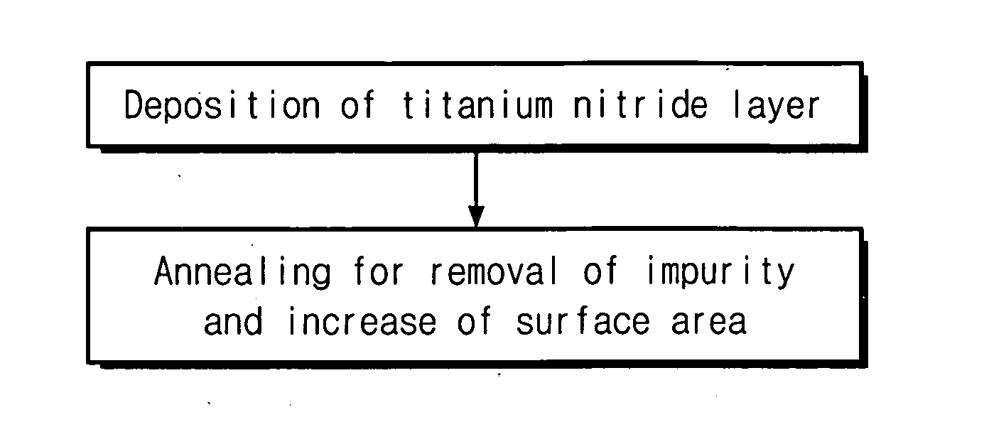
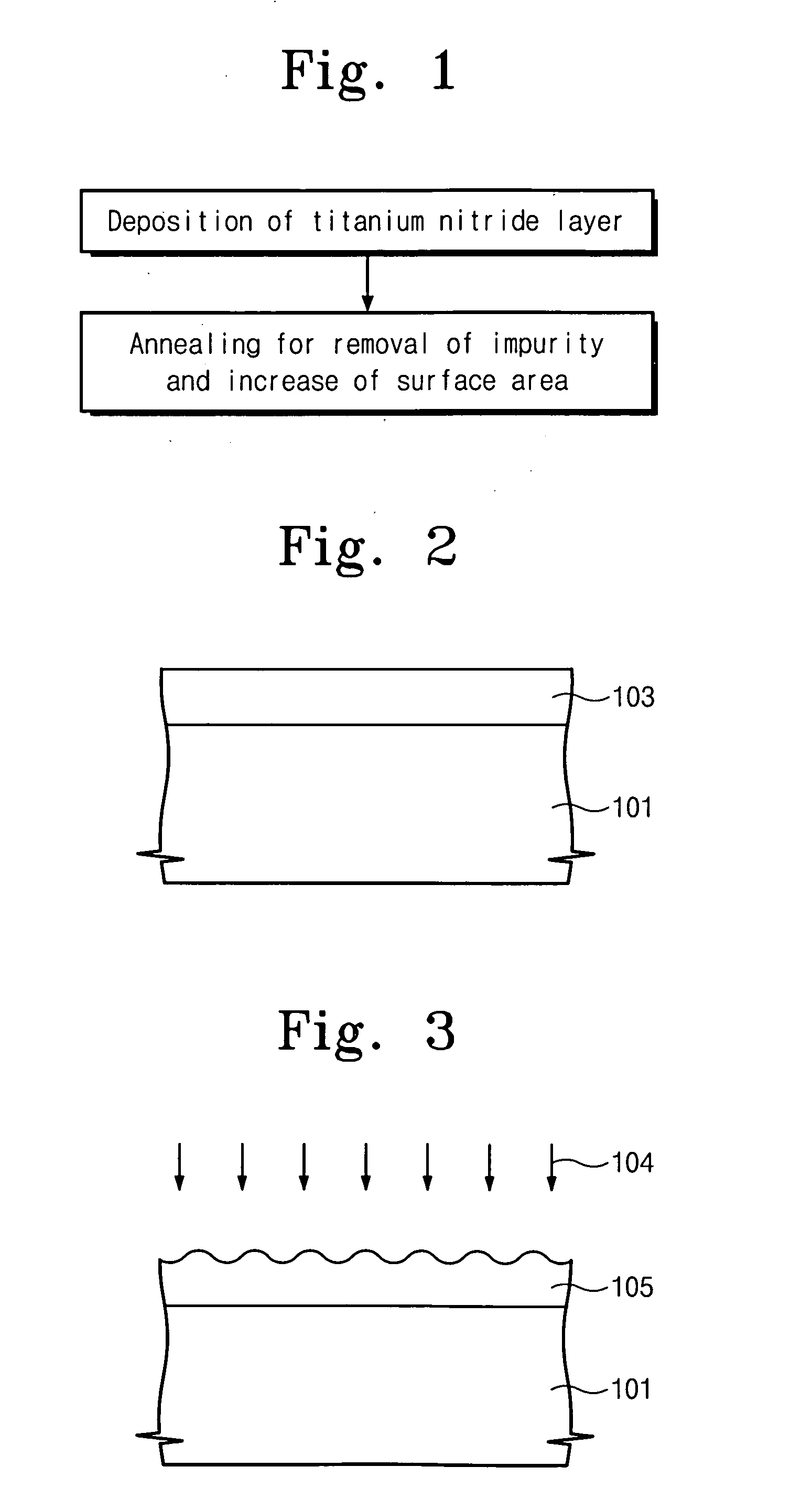
[0028]FIG. 1 is a flow chart of fabrication process illustrating a method for forming a titanium nitride layer according to a preferred embodiment of the present invention.

[0029] The above method comprises: forming a titanium nitride layer by using a metallo-organic chemical vapor deposition (MOCVD) method; then carrying out a rapid thermal process (RTP) on the deposited titanium nitride layer; and during the RTP, removing the residual impurities in the deposited titanium nitride layer and resulting in a soft roughness with increased surface area of the deposited titanium nitride layer.

[0030]FIG. 2 and FIG. 3 show the details...


PUM

PropertyMeasurementUnit
pressureaaaaaaaaaa
temperatureaaaaaaaaaa

Abstract

A method is provided for forming a titanium nitride layer in a metal-insulator-metal (MIM) capacitor. The deposition of a titanium nitride layer is carried out by means of an MOCVD method using a metallo-organic material as a source gas, followed by a rapid thermal process (RTP) at a high temperature. Through the RTP, impurities in the titanium nitride layer are removed and a surface area of the titanium nitride layer is increased in comparison with the titanium nitride layer before the RTP. The titanium nitride layer with increased surface area is useful for a lower electrode of a MIM capacitor.

Description

BACKGROUND OF THE INVENTION [0001] 1. Field of the Invention [0002] The present invention relates to a method for forming a titanium nitride layer, and more particularly, a method for forming a metal-insulator-metal (MIM) capacitor using a titanium nitride layer. [0003] 2. Description of the Related Art [0004] Generally, a capacitor is configured with two conductive electrodes and an insulator interposed in between. The capacitor is a passive element that can store energy in the form of an electrical charge by means of a bias voltage applied to the electrodes. Typically, a single crystalline silicon or a poly-crystalline silicon (hereinafter, referred to as a ‘polysilicon’) is used for the electrodes of the capacitor. The single crystalline silicon or the polysilicon, however, shows a limitation in reducing the resistance of the capacitor electrodes due to its material characteristic. This material characteristic limitation is manifested when a bias voltage is applied to the capacit...

Claims


Application Information

Patent Timeline
Patent Type & Authority Applications(United States)
IPC IPC(8): H01L21/20
CPCC23C16/34H01L2924/0002H01L21/02178H01L21/02181H01L21/022H01L21/0228H01L21/3141H01L21/3142H01L21/31616H01L21/31645H01L21/76843H01L21/76864H01L27/0688C23C16/56H01L2924/00H01L27/04
Inventor KIM, KYONG-MINKIM, DONG-JUNKIM, BYOUNG-DONG
Owner SAMSUNG ELECTRONICS CO LTD
Why Eureka
Try Eureka