Semiconductor die positioning system and a method of bonding a semiconductor die to a substrate

a positioning system and semiconductor technology, applied in the field of semiconductor packaging, can solve the problems of inconvenient assembly, low production yield, inconvenient assembly, etc., and achieve the effects of high fidelity, high fidelity, and reliabl

Inactive Publication Date: 2006-06-22
TRACKING TECH
View PDF26 Cites 2 Cited by
  • Summary
  • Abstract
  • Description
  • Claims
  • Application Information

AI Technical Summary

Benefits of technology

[0009] Accordingly, the present invention includes an efficient, reliable, and easily reproduced die positioning system and a method of making the same. The die positioning system of the present invention includes a substrate having at least one conductive electrical lead thereon and a die positioning structure disposed on the substrate. The die positioning structure is cast and cured specifically for receiving a semiconductor die of the type typically used in...

Problems solved by technology

Nevertheless, a significant and recurring problem faced by semiconductor chip manufacturers is the inaccurate or failed placement of the die in the package.
A misplaced die can render an entire ci...

Method used


Image

  • Semiconductor die positioning system and a method of bonding a semiconductor die to a substrate
  • Semiconductor die positioning system and a method of bonding a semiconductor die to a substrate
  • Semiconductor die positioning system and a method of bonding a semiconductor die to a substrate

Examples


Embodiment Construction

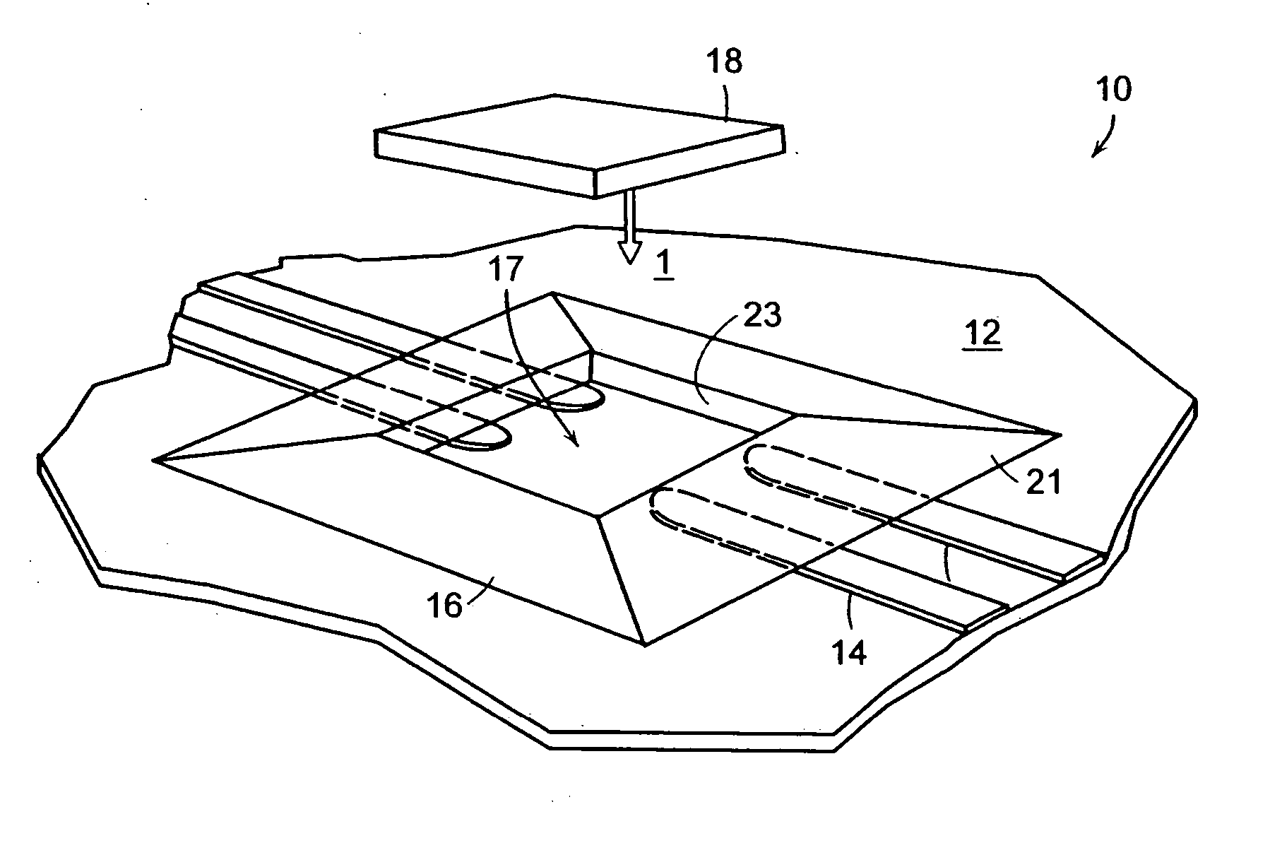
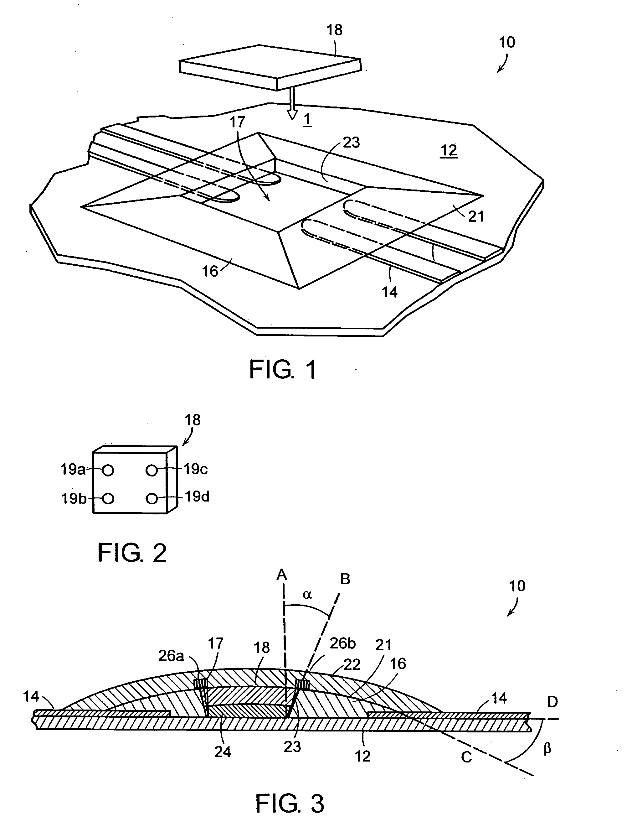
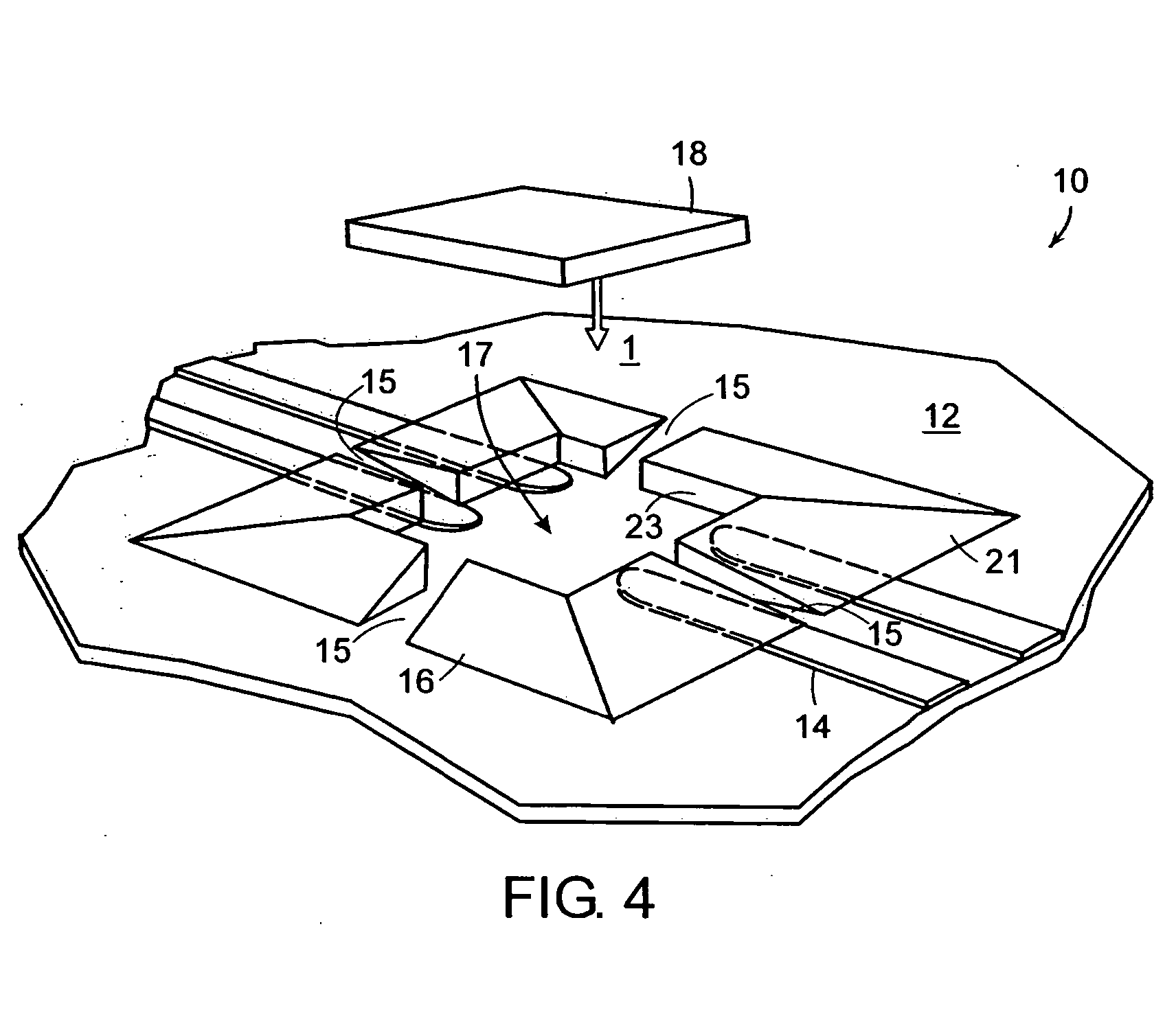
[0021] Two embodiments of the invention to accommodate the semiconductor die in a normal (bond pads up) and flip chip (bond pads down) orientation are presented here.

[0022]FIG. 1 is a perspective view of a die positioning system 10 in accordance with a preferred embodiment of the present invention. The die positioning system 10 includes a substrate 12 having a plurality of electrical leads 14 formed thereon. A die positioning structure 16 is disposed on the substrate 12 and substantially covers the plurality of electrical leads 14. The die positioning structure 16 defines in part an outer slope 21 and an inner slope 23. The die positioning structure 16 also defines a die positioning cavity 17, which allows selective access to the plurality of electrical leads 14. The die positioning cavity 17 is adapted to receive a semiconductor die 18, which may be placed into the die positioning cavity 17 along the direction of arrow 1.

[0023] The substrate 12 should be of low stopping power (su...


PUM


Abstract

The present invention describes a process for bonding a semiconductor die to a selected substrate, including the formation of a die positioning structure on the substrate to receive and secure the semiconductor die. The substrate is selected from a number of materials, the properties of which render it penetrable by electron beam radiation. The die positioning structure is a second material which is electron beam curable, and which is deposited and cured at high speed on the substrate in a novel fashion in accordance with the present invention in a highly efficient reproducible and economical manner.

Description

BACKGROUND OF THE INVENTION [0001] 1. Field of the Invention [0002] The present invention relates generally to the field of semiconductor packaging, and more specifically to the positioning and bonding of a semiconductor die to a selected substrate designated for use in any one of a number of fields, including the manufacture of integrated circuits. [0003] 2. Description of the Related Art [0004] In 1964, Gordon Moore predicted that the number of devices on a single circuit would double every year. This prediction, known as Moore's law, has proven largely accurate, and the resultant growth in the semiconductor industry has been readily apparent. In the early 1960's, the focus of scientists and engineers was on the so-called small-scale integration (SSI), involving between 2 and 50 components per integrated circuit. As of the mid 1990's, the problems to be solved were with regard to ultra large-scale integration (ULSI), involving greater than one million components per integrated cir...

Claims


Application Information

Patent Timeline
IPC IPC(8): H01L23/12H01L21/58
CPCH01L23/13H01L24/80H01L24/81H01L2224/81801H01L2924/01082H01L2924/14H01L2924/19041H01L2924/19043H01L2924/3025H01L2924/01005H01L2924/01006H01L2924/01033H01L2924/12041H01L2924/10253H01L2924/00H01L2224/81136
Inventor CARON, MICHAEL ROGERNABLO, SAMUEL V.FRAZIER, JOHN PAULVOGT, JOHN VINCENT
Owner TRACKING TECH
Why Eureka
Try Eureka