Photomask and method for maintaining optical properties of the same

a photomask and optical technology, applied in the field of semiconductor device manufacturing, can solve the problems of reducing the quality of the photomask, affecting the appearance of the exposed surface, and reducing the optical properties of the same, so as to achieve the effect of substantially reducing or eliminating the disadvantages and problems associated with maintaining the optical properties of the photomask

Inactive Publication Date: 2006-06-22
TOPPAN PHOTOMASKS INC
View PDF7 Cites 12 Cited by
  • Summary
  • Abstract
  • Description
  • Claims
  • Application Information

AI Technical Summary

Benefits of technology

[0006] In accordance with teachings of the present invention, disadvantages and problems associated with maintaining optical properties of a photomask have been substantially reduced or e

Problems solved by technology

As feature sizes of semiconductor devices decrease, the corresponding circuit images on the photomask also become smaller and more complex.
These characteristics may be altered by various procedures during the manufacturing process, which may reduce the quality of the photomask.
The cleaning process, however, can leave a chemical residue on the exposed surfaces.
This residue may react with contaminants that may be created by a lithography system and cause a haze to grow on the exposed surfaces, which may alter the transmission properties of the photomask.
If the transmiss

Method used


Image

  • Photomask and method for maintaining optical properties of the same
  • Photomask and method for maintaining optical properties of the same
  • Photomask and method for maintaining optical properties of the same

Examples


Embodiment Construction

[0017] Preferred embodiments of the present invention and their advantages are best understood by reference to FIGS. 1 through 3, where like numbers are used to indicate like and corresponding parts.

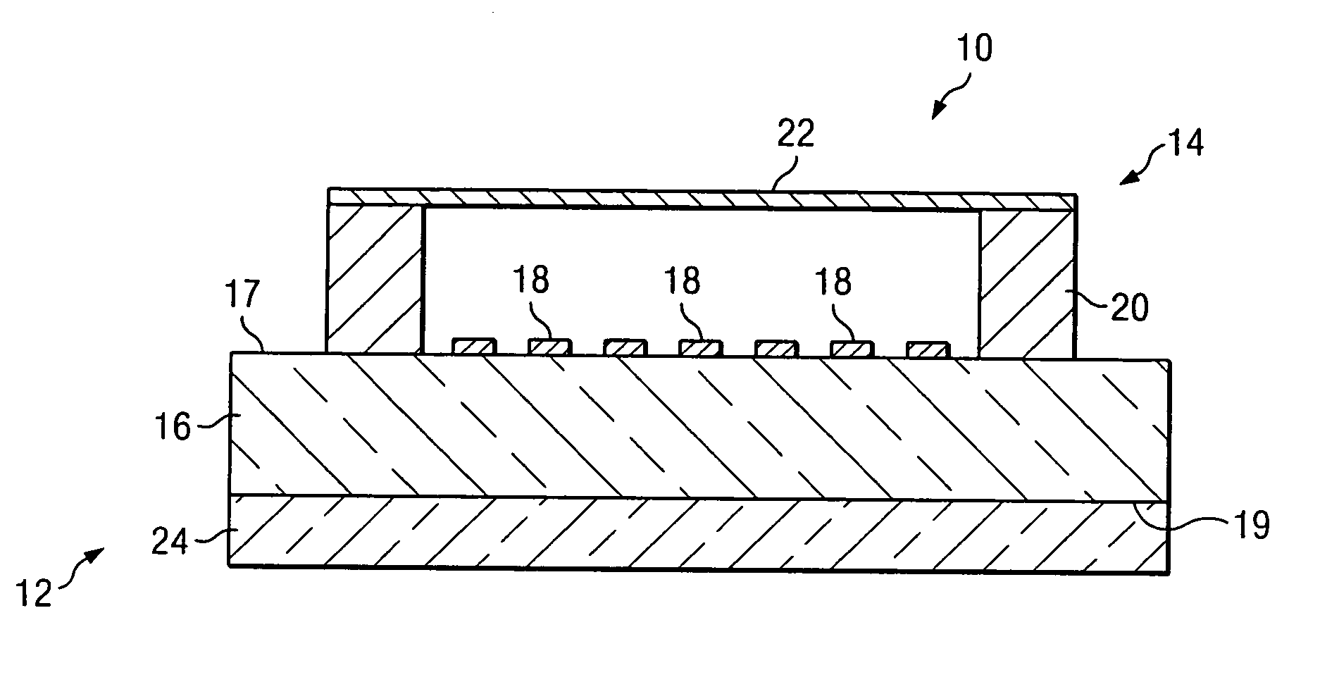
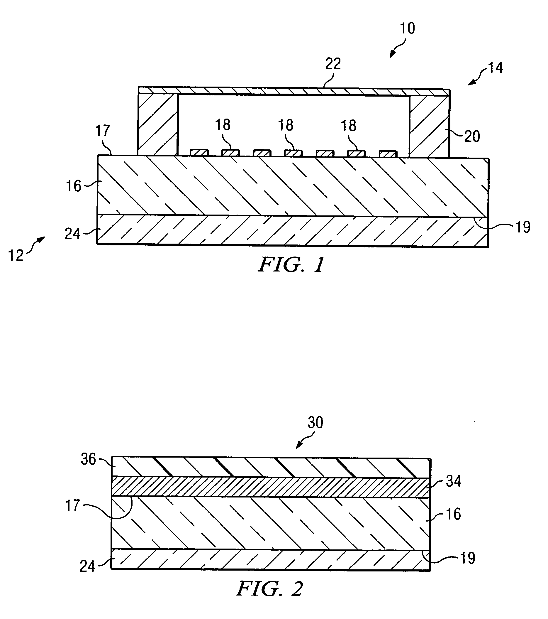
[0018]FIG. 1 illustrates a cross-sectional view of a photomask assembly including a protective layer formed on at least one surface of the substrate. Photomask assembly 10 includes pellicle assembly 14 mounted on photomask 12. Substrate 16 and patterned layer 18 form photomask 12, also known as a mask or reticle, that may have a variety of sizes and shapes, including but not limited to round, rectangular, or square. Photomask 12 may also be any variety of photomask types, including, but not limited to, a one-time master, a five-inch reticle, a six-inch reticle, a nine-inch reticle or any other appropriately sized reticle that may be used to project an image of a circuit pattern onto a semiconductor wafer. Photomask 12 may further be a binary mask, a phase shift mask (PSM) (e.g., an alte...


PUM


Abstract

A photomask and method for maintaining optical properties of the same are disclosed. The method includes providing a substrate including a first surface having an absorber layer formed thereon and a second surface located opposite the first surface. A pattern is formed in the absorber layer to create a photomask for use in a semiconductor manufacturing process. A transmissive protective layer is also formed on at least one of the patterned layer and the second surface of the substrate. The protective layer reduces haze growth when the photomask is used in the semiconductor manufacturing process.

Description

RELATED APPLICATION [0001] This application is a Continuation of International Patent Application No. PCT / US04 / 27435 filed Aug. 24, 2004, which designates the United States and claims the benefit of U.S. Provisional Patent Application Ser. No. 60 / 497,541, entitled “Photomask and Method for Maintaining Optical Properties of the Same” filed by Laurent Dieu et al. on Aug. 25, 2003, which are incorporated herein by reference in their entirety.TECHNICAL FIELD OF THE INVENTION [0002] The present invention relates in general to semiconductor device manufacturing and, more particularly to a photomask and method for maintaining optical properties of the same. BACKGROUND OF THE INVENTION [0003] As semiconductor device manufacturers continue to produce smaller devices, the requirements for photomasks used in the fabrication of these devices continue to tighten. Photomasks, also known as reticles or masks, typically consist of substrates (e.g., high-purity quartz or glass) that have an opaque a...

Claims


Application Information

Patent Timeline
IPC IPC(8): B08B7/00B08B6/00G21G5/00G03C5/00G03F1/00B08B3/12B08B7/02A61N5/00G03FG03F1/14G03F9/00
CPCG03F1/48
Inventor DIEU, LAURENTGORDON, JOSEPH STEPHENJOHNSTONE, ERIC VINCENTCHOVINO, CHRISTIAN
Owner TOPPAN PHOTOMASKS INC
Why Eureka
Try Eureka