Encapsulation and packaging of ultraviolet and deep-ultraviolet light emitting diodes

Inactive Publication Date: 2006-06-29
III N TECH
View PDF10 Cites 172 Cited by
  • Summary
  • Abstract
  • Description
  • Claims
  • Application Information

AI Technical Summary

Benefits of technology

[0018] These new LEDs will also be medically useful. The compact nature of the UV or DUV LED light sources makes them ideal for medical research and surgical procedures. Some foreseen examples include the miniaturizati

Problems solved by technology

The FIG. 1—type arrangement, however, does not work with some newly-developed LEDs.
One of the serious problems related with high-efficiency LEDs is the occurrence of generated light trapped in the high refractive index semiconductor itself without emitting out.
With the development of blue and near-UV LEDs and power white LEDs in recent years, however, the traditional epoxy-resin encapsulation has not worked so well.
It has been discovered that—when using these new LED types—thermal aging and high-energy (short wavelength) photon absorption cause a yellowish phenomenon to occur in the traditional epoxy resin encapsulation.
This dramatically degrades transparency, thus inhibiting light transmission.
But these alternatives are limited in that they are transmission-inhibited with respect to light wavelengths below 400 nm and have cut-off wavelengths well above 300 nm (depending on composition).
Further, the absorption of short-wavelength (λ<360 nm) UV and DUV light will dramatically degrade their performance.
With respect to UV and DUV LEDs, there are currently no acceptable options with respect to encapsulation and packaging.
This greatly

Method used


Image

  • Encapsulation and packaging of ultraviolet and deep-ultraviolet light emitting diodes
  • Encapsulation and packaging of ultraviolet and deep-ultraviolet light emitting diodes
  • Encapsulation and packaging of ultraviolet and deep-ultraviolet light emitting diodes

Examples


first embodiment

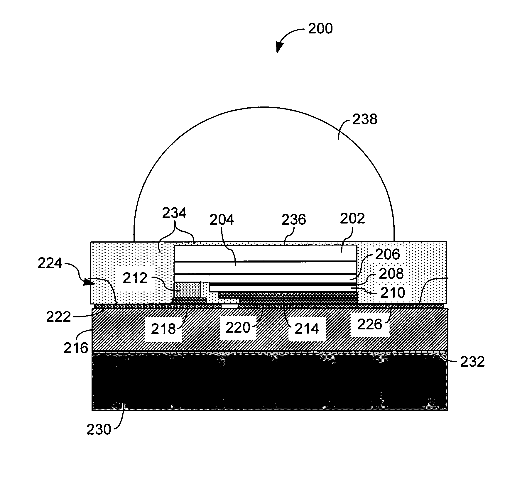
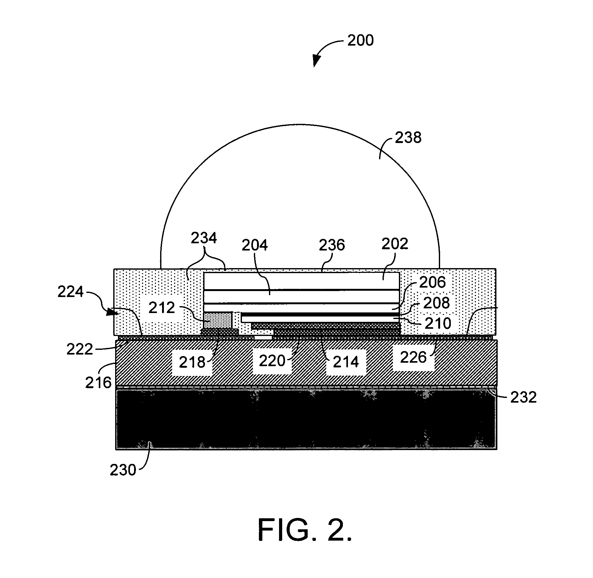
[0029]FIG. 2 illustrates the invention. Disclosed in the figure is an AlGaN (or AlInGaN) based UV / DUV LED structure 200. LED 200 includes a substrate 202, an AIN epilayer 204, an AlGaN n-type material layer 206, an AlGaN (or AlInGaN) active region 208, and an AlGaN p-type material layer 210. It will be apparent to one skilled in the art that alternative materials may be substituted for those disclosed here to comprise the various layers. Thus, the scope of the present invention is not be limited to the particular materials used in this disclosed embodiment here.

[0030] The semiconductor layers in FIG. 2 are epitaxially grown on substrate 202 (for which transparent sapphire is the most common choice). An n-contact 212 and a p-contact 214 form the electrical connections to the n-type AlGaN layer 206 and p-type AlGaN layer 210, respectively. As will be recognizable to one skilled in the art, contacts 212 and 214 may thus be used to create voltage across the LED for injecting electrons a...

embodiment 600

[0045] The encapsulation and packaging techniques of the present invention also are adaptable for UV / DUV LEDs packaging without flip-chip bonding. Direct bonding is also possible. Such an embodiment is shown in FIG. 6. The FIG. 6 embodiment is similar to the flip-chip bonded packaging in FIG. 4, except that it is a direct-LED-die attachment embodiment 600. The figure shows a UV / DUV LED 602 with epi-layers facing up. The LED is mounted on a substrate 604. Substrate 604 is directly bonded on a metal slug 608 of the packaging house with a solder or thermal paste 606, and an n- and p-contact pair is wire-bonded (via a wire pair 616) to an electrical lead pair (610 and 612) of the package. An encapsulation dome 618 is directly formed in the package house cavity with polymer resins, just like with the FIG. 4 embodiment. Also like the FIG. 4 embodiment, a dual-tiered side wall arrangement 614 is employed.

[0046] The same materials suggested for the FIG. 4 embodiment may be used for the FIG....


PUM


Abstract

Disclosed are the materials and methods used to package and encapsulate UV and DUV LEDs. These LEDs have emission wavelengths in the range from around 360 nm to around 200 nm. The UV/DUV LED die or its flip-chip bonded subassembly are disposed in a low thermal resistance packaging house. Either the whole package or just the UV/DUV LED is globed with a UV/DUV transparent dome-shape encapsulation. This protects the device, enhances light extraction, and focuses the light emitted. The dome-shape encapsulation may be comprised of optically transparent PMMA, fluorinated polymers or other organic materials. Alternatively it might be configured having a lens made from sapphire, fused silica or other transparent materials. The lens material is cemented on the UV/DUV LED with UV/DUV transparent polymers.

Description

BACKGROUND OF THE INVENTION [0001] 1. Field of the Invention [0002] The present invention relates to the encapsulation and packaging of ultraviolet (UV) and deep-ultraviolet (DUV) light emitting diodes (LEDs) semiconductor devices, especially those with emitting wavelengths between around 360 nm and 200 nm. [0003] 2. Description of the Prior Art [0004] The advances in III-nitride semiconductors (including GaN, InN, AlN, and their alloys), especially those used in high Al-content AlGaN and AlInGaN based light emitting diode (LED) technologies, allow for the first time to push the emitting wavelength of the semiconductor LED to the UV and DUV range. These new semiconductors, depending on Al content, have a bandgap up to 6.2 eV, which corresponds to an emitting wavelength down to 200 nm, covering the near-UV, UV, and DUV range. [0005] The conventional LEDs based on GaAs, InP, or even InGaN, emit a wavelength in the visible to near infrared (IR) range. For these visible or near-IR LEDs,...

Claims


Application Information

Patent Timeline
IPC IPC(8): H01L33/00H01L29/24H01L33/56H01L33/58
CPCH01L33/56H01L33/58H01L2224/48247H01L2924/01322H01L2924/00H01L2924/181H01L2224/48091H01L2924/00012H01L2924/00014
Inventor FAN, ZHAOYANGJIANG, HONGXINGLIN, JINGYU
Owner III N TECH
Why Eureka
Try Eureka