CMOS image sensor and method for fabricating the same

a technology of image sensor and manufacturing method, which is applied in the field of image sensor, can solve the problems of complex fabrication process requiring multi-phase photo process, high power consumption, and complicated driving method, and achieve the effect of eliminating the thickness of the planarization layer and improving image characteristics

Active Publication Date: 2006-06-29
CONVERSANT INTPROP MANAGEMENT INC
View PDF12 Cites 49 Cited by
  • Summary
  • Abstract
  • Description
  • Claims
  • Application Information

AI Technical Summary

Benefits of technology

[0016] An advantage of the present invention is to provide a CMOS image sensor and a method for fabricating the same that improves image characteristics by eliminating the thickness of a planarization layer.
[0017] Additional features and advantages of the invention will be set forth in the description which follows, and in part will be apparent from the description, or may be learned by practice of the invention. The objectives and other advantages of the invention will be realized and attained by the structure particularly pointed out in the written description and claims hereof as well as the appended drawings.
[0018] To achieve these and other advantages and in accordance with the purpose of the present invention, as embodied and broadly described, there is provided a CMOS image sensor comprising a semiconductor substrate; a plurality of active devices, provided in a predetermined surface of the semiconductor substrate, for generating electrical charges according to an amount of incident light; an insulating interlayer formed on an entire surface of the semiconductor substrate including the plurality of active devices; a color filter layer formed on the insulating interlayer, the color filter layer comprised of red, green, and blue color filter patterns for respectively filtering light according to wavelength, the color filter patterns arranged to correspond to the plurality of active devices; and a plurality of microlenses formed on the color filter layer, wherein the color filter layer is planarized so that each color filter pattern of the color filter layer is imparted with an equal height for receiving the plurality of microlenses.
[0019] In another aspect of the present invention, there is provided a method for fabricating a CMOS image sensor. The method comprises forming a plurality of photodiodes in a predetermined surface of a semiconductor substrate; forming an insulating interlayer on an entire surface of the semiconductor substrate including the plurality of photodiodes; forming a color filter layer including red, green, and blue color filter patterns on the insulating interlayer; planarizing the color filter layer so that each color filter pattern of the color filter layer is imparted with an equal height; and forming a plurality of microlenses on the planarized color filter layer.
[0020] It is to be understood that both the foregoing general description and the following detailed description are exemplary and explanatory and are intended to provide further explanation of the invention as claimed.

Problems solved by technology

Disadvantages of a charge-coupled device include a complicated driving method, high power consumption, and a complicated fabrication process requiring a multi-phased photo process.
In a charge-coupled device, integration of complementary circuitry such as a control circuit, a signal processor, and an analog-to-digital converter into a single-chip device is difficult.
Thus, development of compact-sized or thin products using such image sensors is hindered.
However, there is a limit to increasing the photo-sensing portion due to the required presence of the logic circuit portion.
The pattern profile or shape of the microlens tends to vary according to exposure conditions, for example, the conditions of a thin film on the semiconductor substrate, which are rather unstable.
This results in degraded focusing characteristics.
Since the light-receiving efficiency of the CMOS image sensor of the related art depends on the amount of light reaching the photodiode, light sensitivity is lowered due to the greater traveling distance, thereby deteriorating the capacity of the CMOS image sensor.

Method used


Image

  • CMOS image sensor and method for fabricating the same
  • CMOS image sensor and method for fabricating the same
  • CMOS image sensor and method for fabricating the same

Examples


Embodiment Construction

[0028] Reference will now be made in detail to embodiments of the present invention, examples of which are illustrated in the accompanying drawings. Wherever possible, like reference designations will be used throughout the drawings to refer to the same or similar parts.

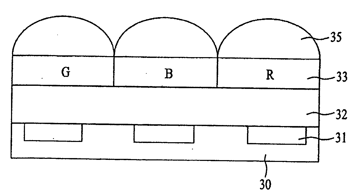
[0029] An embodiment of the present invention will be described with reference to FIG. 4A-5C. As shown in FIG. 4A, a plurality of photodiodes 41, which may be in the form of a plurality of photo-gates, are formed at fixed intervals in a predetermined surface of a semiconductor substrate 40. Then, an insulating interlayer 42 of an oxide such as undoped silicate glass is formed on an entire surface of the semiconductor substrate 40 including the plurality of photodiodes 41. The insulating interlayer 42 may be formed as a multi-layered structure, including a light-shielding layer (not shown) for preventing light from reaching areas other than the photodiodes 41, and another insulating interlayer (not shown) formed on t...


PUM


Abstract

A CMOS image sensor and method for fabricating the same improve image characteristics by eliminating the thickness of a planarization layer. The CMOS image sensor includes a semiconductor substrate; a plurality of active devices, provided in a predetermined surface of the semiconductor substrate, for generating electrical charges according to an amount of incident light; an insulating interlayer formed on an entire surface of the semiconductor substrate including the plurality of active devices; a color filter layer formed on the insulating interlayer, the color filter layer comprised of red, green, and blue color filter patterns for respectively filtering light according to wavelength, the color filter patterns arranged to correspond to the plurality of active devices; and a plurality of microlenses formed on the color filter layer, wherein the color filter layer is planarized so that each color filter pattern of the color filter layer is imparted with an equal height for receiving the plurality of microlenses.

Description

CROSS-REFERENCE TO RELATED APPLICATIONS [0001] This application claims the benefit of Korean Patent Application No. 10-2004-0114658 filed on Dec. 29, 2004, which is hereby incorporated by reference for all purposes as if fully set forth herein. BACKGROUND OF THE INVENTION [0002] 1. Field of the Invention [0003] The present invention relates to an image sensor, and more particularly, to a CMOS image sensor and a method for fabricating the same, which improves the sensor's image characteristics. [0004] 2. Discussion of the Related Art [0005] Image sensors are semiconductor devices for converting an optical image into an electrical signal and include charge-coupled devices and complementary metal-oxide-semiconductor (CMOS) image sensors. A general charge-coupled device includes an array of photodiodes converting light signals into electrical signals. Disadvantages of a charge-coupled device include a complicated driving method, high power consumption, and a complicated fabrication proc...

Claims


Application Information

Patent Timeline
Patent Type & Authority Applications(United States)
IPC IPC(8): H01L31/062H01L21/00
CPCH01L27/14621H01L27/14627H01L27/14685H01L27/146H01L31/10
Inventor KIM, SEOUNG HYUN
Owner CONVERSANT INTPROP MANAGEMENT INC
Why Eureka
Try Eureka