Semiconductor device and fabrication method thereof

a semiconductor device and semiconductor technology, applied in semiconductor devices, semiconductor/solid-state device details, electrical devices, etc., can solve the problems of occupying a large amount of total thickness (e.g., 30%) of the semiconductor device, and the resin layer is nearly as thick, so as to simplify the formation of the opening and the thickness of the protective layer

Inactive Publication Date: 2006-06-29
LAPIS SEMICON CO LTD
View PDF5 Cites 44 Cited by
  • Summary
  • Abstract
  • Description
  • Claims
  • Application Information

AI Technical Summary

Benefits of technology

[0010] This structure enables the thickness of the protective layer (the package layer in a wafer level chip size package) to be reduced because the electrode is connected directly to the conductive pattern. The protective layer may comprise a photosensitive material, which simplifies the formation of the opening for the electrode.

Problems solved by technology

A problem with this process is that even after polishing, the resin layer is nearly as thick (e.g., 90 μm thick) as the original height of the posts, and takes up much of the total thickness (e.g., 30%) of the semiconductor device.

Method used


Image

  • Semiconductor device and fabrication method thereof
  • Semiconductor device and fabrication method thereof
  • Semiconductor device and fabrication method thereof

Examples


first embodiment

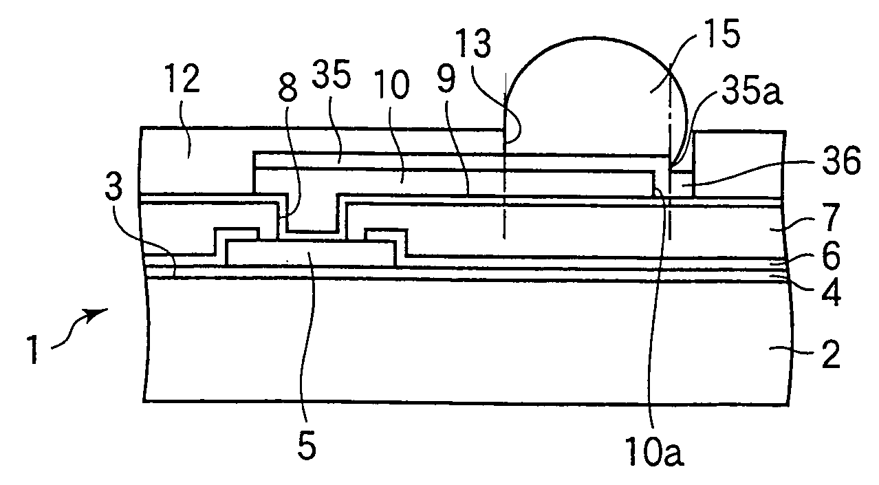
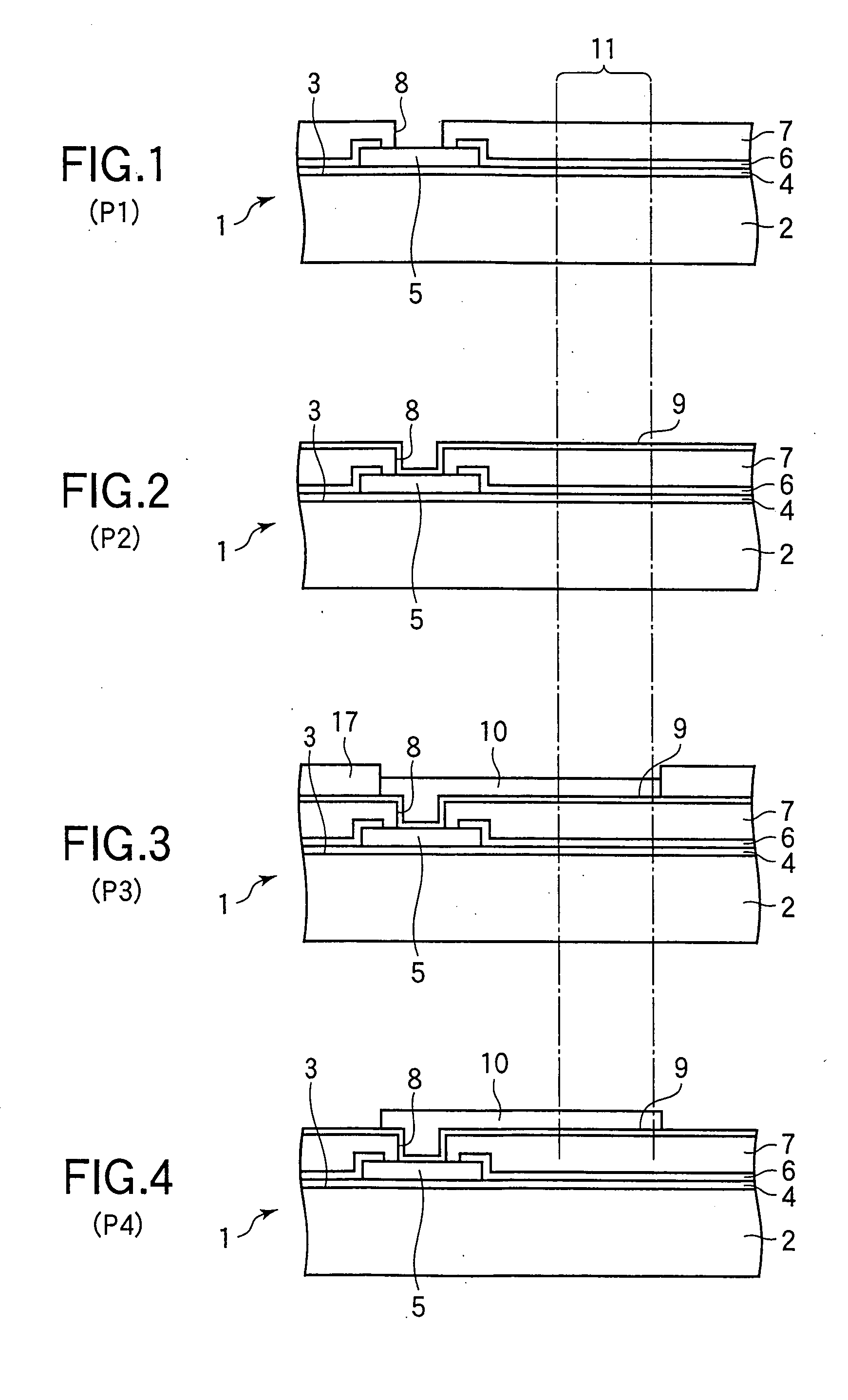
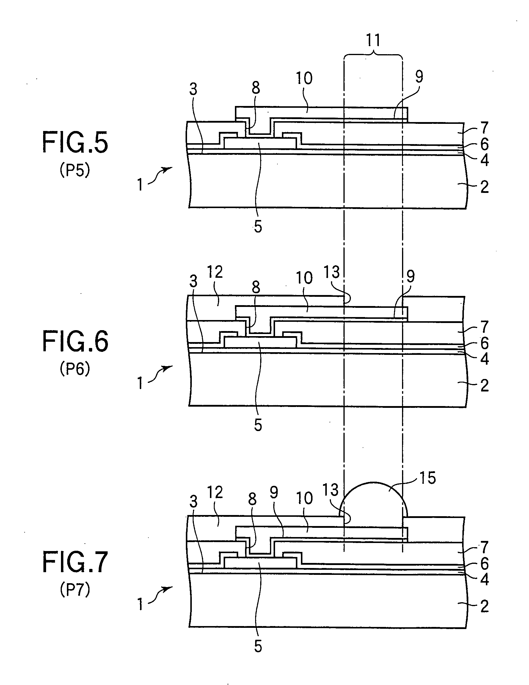
[0022] The first embodiment is a semiconductor device fabricated from a wafer 1 as illustrated in FIGS. 1 to 7.

[0023] The semiconductor wafer 1 includes a semiconductor substrate 2 having a front surface (the first surface, the upper surface in the drawings) and a back surface (the second surface, the lower surface in the drawings). The front surface is also referred to as the circuit surface 3, because it includes a plurality of interconnected circuit elements such as transistors (not shown). The circuit surface 3 is covered by a dielectric layer 4 of silicon dioxide with openings referred to as contact holes (not shown) leading to circuit elements on the circuit surface 3. The surface of the dielectric layer 4 is covered with a conductive metal film such as an aluminum film (not shown). The metal is patterned to form interconnection wiring (not shown) that is electrically coupled to the circuitry on the circuit surface 3 through the contact holes.

[0024] Patterning of the conduct...

second embodiment

[0043] The second embodiment is a semiconductor device fabricated from a wafer 1 as illustrated in FIGS. 8 to 15.

[0044] The second embodiment differs from the first embodiment by including conductive nubs referred to below as redistribution nubs 21, seen in FIGS. 12 to 15. The redistribution nubs 21 are cylindrical projections of the same material as the redistribution-pattern 10, and are formed in the electrode areas 11, making direct electrical contact with the redistribution pattern 10.

[0045] A fabrication method for the semiconductor device in the second embodiment includes the steps PA1 to PA8 illustrated in FIGS. 8 to 15.

[0046] Since steps PA1 to PA4 in FIGS. 8.to 11 are the same as steps P1 to P4 in FIGS. 1 to 4 in the first embodiment, descriptions will be omitted.

[0047] In step PA5 in FIG. 12, a second photoresist mask 17 is formed (this photoresist mask is different from the photoresist mask used in step PA3 in FIG. 10). The second photoresist mask 17 covers all parts ...

third embodiment

[0056] The third embodiment is a semiconductor device fabricated from a wafer 1 as illustrated in FIGS. 16 to 25.

[0057] The third embodiment differs from the first embodiment by including a second metal underlayer 23 and conductive redistribution nubs 24. In FIG. 22, the second metal underlayer 23 is deposited as a multilayer film on the entire front surface of the protective layer 12 by sputtering, as was the metal underlayer 9 in the first embodiment, and is patterned by etching to cover the edges of the electrode openings 13 in the protective layer 12, the exposed parts of redistribution pattern 10 at the bottom of the electrode openings 13, and the inner walls of the electrode openings 13.

[0058] The conductive redistribution nubs 24 are generally cylindrical projections of the same material as the redistribution pattern 10. The conductive redistribution nubs 24 have large-diameter and small-diameter parts, and are formed on the electrode areas 11, making direct electrical cont...


PUM

PropertyMeasurementUnit
heightaaaaaaaaaa
diameteraaaaaaaaaa
thickaaaaaaaaaa

Abstract

A semiconductor device includes a semiconductor substrate with circuit elements and electrode pads formed on one surface. This surface is covered by a dielectric layer with openings above the electrode pads. A metal layer is deposited on the dielectric layer and patterned to form a conductive pattern with traces leading to the electrode pads. A protective layer having openings exposing part of the conductive pattern is formed. Each opening is covered by an electrode such as a solder bump, which is electrically connected through the conductive pattern to one of the electrode pads. This structure enables the thickness of the protective layer, which may function as a package of the semiconductor device, to be reduced. The protective layer may be formed from a photosensitive material, simplifying the formation of the openings for the electrodes.

Description

BACKGROUND OF THE INVENTION [0001] 1. Field of the Invention [0002] The present invention relates to a small semiconductor device such as a device with a wafer level chip size package, and to the fabrication of this type of semiconductor device, more particularly to the fabrication of electrodes on the surface of the package and their interconnections to pads on the semiconductor device within the package. [0003] 2. Description of the Related Art [0004] With the recent rising demand for smaller, slimmer semiconductor integrated circuits, wafer level chip size packages have become prevalent, especially for thin semiconductor devices. A wafer level chip size package (WCSP) is simply a protective layer with a grid of hemispherical bump electrodes, formed on a semiconductor integrated circuit in the wafer processing stage before the wafer is diced into individual integrated circuit chips. WCSP semiconductor devices as thin as three-tenths of a millimeter (0.3 mm) have been developed. [0...

Claims


Application Information

Patent Timeline
Patent Type & Authority Applications(United States)
IPC IPC(8): H01L23/48
CPCH01L23/3114H01L2924/0002H01L2224/1147H01L2224/1148H01L2224/1191H01L2224/13099H01L2924/01013H01L2924/01015H01L2924/01029H01L2924/01046H01L2924/01075H01L2924/01079H01L2924/01082H01L2924/14H01L2224/05569H01L2224/13005H01L2224/023H01L2224/05541H01L2224/05548H01L2224/13022H01L2224/13023H01L2224/13027H01L2924/01006H01L2924/01033H01L2924/014H01L2224/13006H01L2224/05572H01L2224/0231H01L2924/00014H01L24/13H01L24/11H01L2224/11334H01L2224/0401H01L23/49816H01L2924/207H01L2924/00H01L2224/05552H01L2224/11H01L2224/13H01L2224/05124H01L2224/05147H01L2224/05644H01L2224/05647H01L2224/05655H01L2224/05664H01L24/05H01L2924/0001H01L2224/13024H01L24/02H01L2224/02
Inventor WATANABE, KIYONORI
Owner LAPIS SEMICON CO LTD
Why Eureka
Try Eureka