Method for etching and for forming a contact hole using thereof

a technology of contact hole and etching, which is applied in the direction of basic electric elements, semiconductor/solid-state device manufacturing, electric devices, etc., can solve the problems of increasing manufacturing costs, increasing manufacturing costs, and uneven degree of tapering of photo resist patterns after thermal reflow, so as to suppress the increase of manufacturing processes, increase of manufacturing costs, and increase of manufacturing costs

Inactive Publication Date: 2006-06-29
VISTA PEAK VENTURES LLC
View PDF1 Cites 8 Cited by
  • Summary
  • Abstract
  • Description
  • Claims
  • Application Information

AI Technical Summary

Benefits of technology

[0051] Namely, the object of the present invention is to provide a method for forming an etching structure without difficulty to control the manufacturing conditions, and with a minute dimension exceeding the limit of exposure, while suppressing increase of manufacturing processes and increasing of manufacturing cost.
[0052] Another object of the present invention is to provide a method for forming a plurality of etching structures with different depth without over etching in one time process of lithography, while suppressing increase of manufacturing processes and increasing of manufacturing cost.
[0053] Still another object of the present invention is to provide a method for forming an etching structure with largely inclined and forward tapered shape, while suppressing increase of manufacturing processes and increasing of manufacturing cost.
[0054] Further, the object of the present invention is to provide a method for forming a contact hole without difficulty to control the manufacturing conditions, and with a minute dimension exceeding the limit of exposure, while suppressing increase of manufacturing processes and increasing of manufacturing cost.
[0055] Another object of the present invention is to provide a A method for forming a plurality of contact holes with different depth without over etching in one time process of lithography, while suppressing increase of manufacturing processes and increasing of manufacturing cost.
[0056] Still another object of the present invention is to provide a method for forming contact hole with largely inclined and forward tapered shape, while suppressing increase of manufacturing processes and increasing of manufacturing cost.

Problems solved by technology

However, as thus high performance of the semiconductor device progresses, it follows that the manufacturing cost increases because of sophisticated manufacturing processes.
However, the first prior art making use of the thermal reflow includes the following drawback.
1) The first problem is that in case of unevenness in the photo resist width, the degree of tapering in photo resist patterns after the thermal reflow becomes uneven because the shape at the reflow portion depends on the width of photo resist patterns.
2) The second problem is that tapering by thermal reflow involves diminishing of the dimension of the photo resist pattern in the horizontal direction.
Namely, there exists a limitation in increasing the dimension in the horizontal direction, because the thermal reflow causes contraction in volume of the organic pattern due to heat, in addition to increase of the dimension in the horizontal direction due to fluidization.
3) The third problem is that because the thermal reflow is a reflow with high viscosity, the front shape of the reflow becomes undulant and uneven, and as the result, such mask due to the thermal reflow for etching allows often to form side etching, thereby causing wiring with inadequate tapered shape, that is, the cross section of the wiring with the shape of vertical or partially reverse tapered.
However, the second prior art includes the following drawback.
Namely, the degree of angle of the tapered shape in the contact hole with the forward tapered shape due to the second prior art is only a little, and therefore it is impossible for the second prior art to be applied to forming a contact hole necessary for a large or significant forward tapering.
However, the third prior art includes the following drawback.
As stated previously, because the shallow contact hole is exposed through over etching the following two problems arise.
The first problem is that the surface of the second electrode to which the shallow contact hole reaches is subjected to heavy damage by over etching, and later that causes burnout failure in the second wiring lying with the spread on the surface of the second electrode and along the side wall of the shallow contact hole, and causes increase of contact resistance between the second wiring and the surface of the second electrode.
The second problem is that forming forward tapered shape of the contact hole becomes difficult.
However, the fourth prior art, though it makes use of the half exposure technology, still includes the following drawback.
Accordingly, the number of processes for manufacturing increases, compared with the ordinary cases in which a resist mask is made of the same film thickness, and then the manufacturing cost increases.
Also, further processes are required to remove the thin portion in film, thickness of the resist mask and then to form the second opening portion that leads to increase of the number of manufacturing process and the cost.

Method used


Image

  • Method for etching and for forming a contact hole using thereof
  • Method for etching and for forming a contact hole using thereof
  • Method for etching and for forming a contact hole using thereof

Examples


embodiment 1

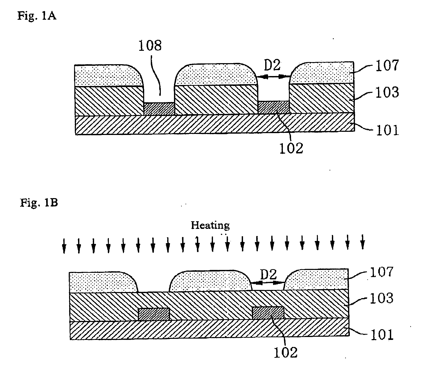
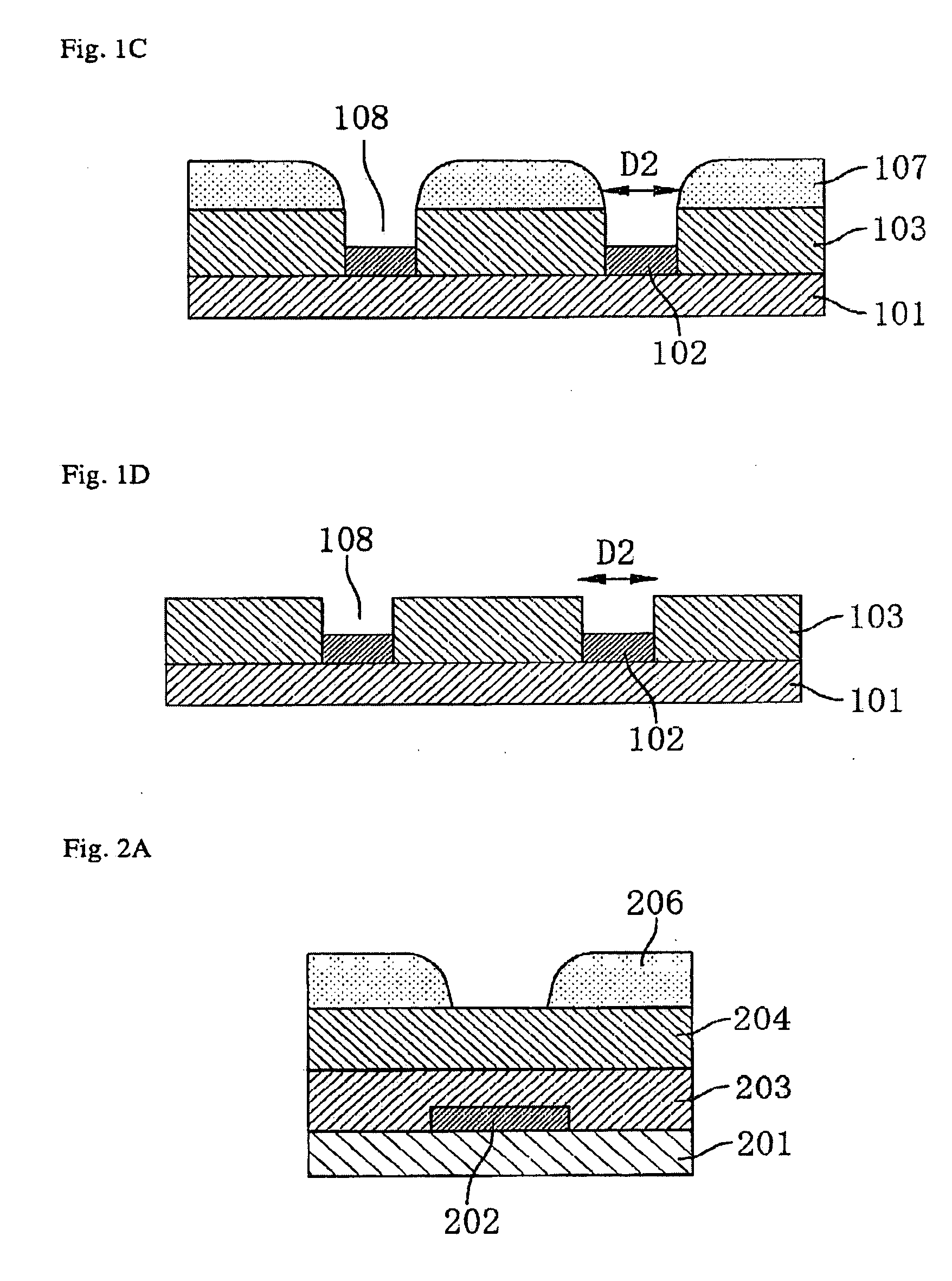
[0196] Embodiment 1 will be explained below. The embodiment 1 corresponds to the typical example that conducts the first to the third aspects of the present invention. FIGS. 4A to 4E illustrate longitudinal cross sectional views showing a series of processes forming a plurality of holes with different depth through one time process of the lithography with regard to the embodiment 1 of the present invention.

[0197] As illustrated in FIG. 4A, a first conductive constituent part 2 is selectively formed on a substrate 1. The substrate 1 can be formed with an insulating substrate. The insulating substrate may be, for example, a transparent substrate such as glasses for the use of the liquid crystal display device, and insulating films such as amorphous silicon, silicon dioxide films, silicon nitride films, silicon dioxide films and silicon nitride films for the use of semiconductor integrated circuits. In addition the first conductive constituent part 2 can be formed with a conductive fi...

embodiment 2

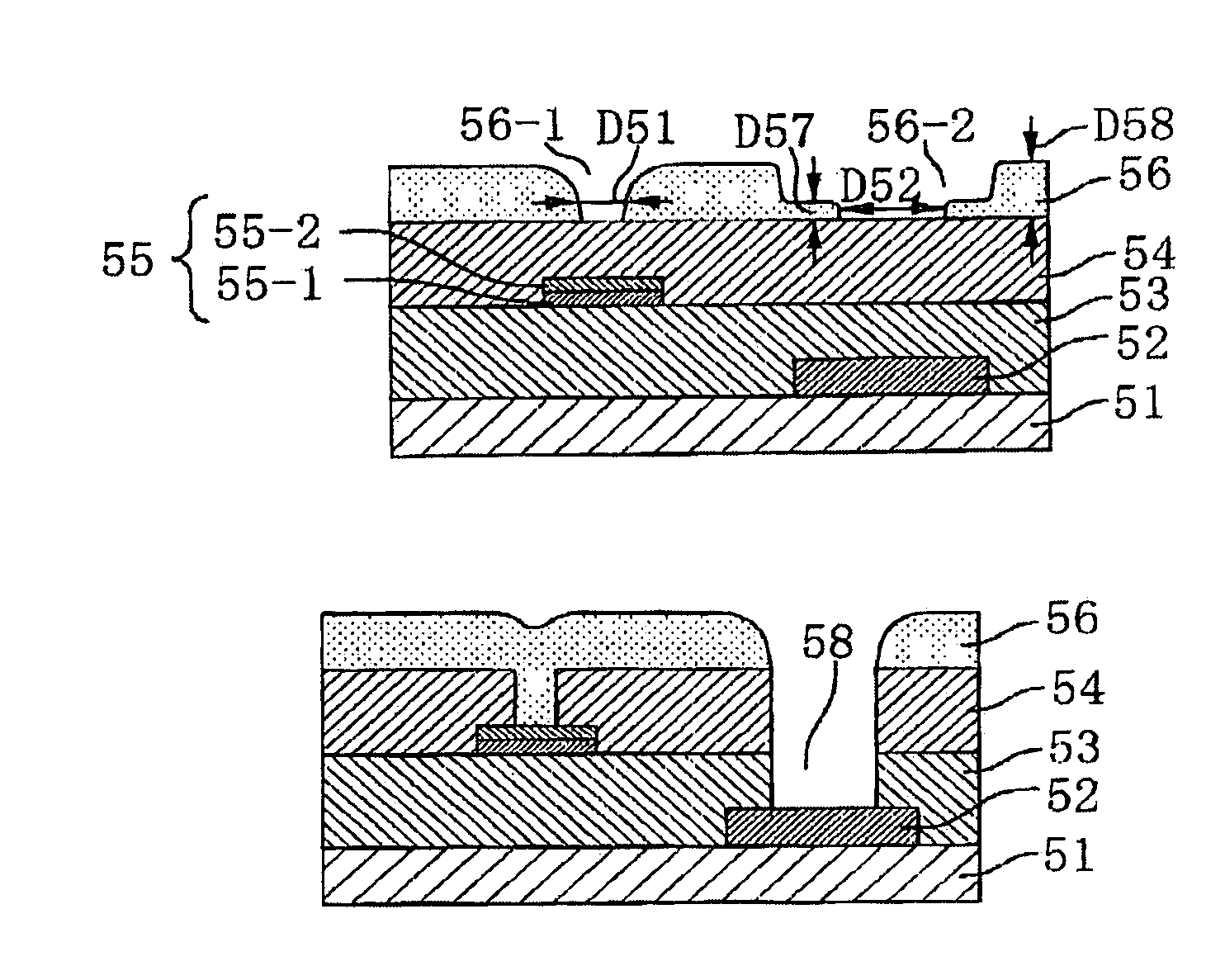
[0219] Embodiment 2 will be explained below. The embodiment 2 corresponds to the typical example that conducts the second, the fourth and the fifth aspects of the present invention. FIGS. 5A to 5E illustrate longitudinal cross sectional views showing a series of processes forming a plurality of holes with different depth through one time process of the lithography with regard to the embodiment 2 of the present invention.

[0220] As illustrated in. FIG. 5A, a first conductive constituent part 52 is selectively formed on a substrate 51. The substrate 51 can be formed with an insulating substrate. The insulating substrate may be, for example, a transparent substrate such as glasses for the use of the liquid crystal display device, and insulating films such as amorphous silicon, silicon dioxide films, silicon nitride films, silicon dioxide films and silicon nitride films for the use of semiconductor integrated circuits. In addition the first conductive constituent part 52 can be formed w...

embodiment 3

[0244] Embodiment 3 will be explained below. The embodiment 3 corresponds to the typical example that conducts the second, the fourth and the sixth aspects of the present invention. FIGS. 6A to 6F illustrate longitudinal cross sectional views showing a series of processes forming a plurality of holes with different depth through one time process of the lithography with regard to the embodiment 3 of the present invention.

[0245] As illustrated in FIG. 6A, a first conductive constituent part 72 is selectively formed on a substrate 71. The substrate 71 can be formed with an insulating substrate. The insulating substrate may be, for example, a transparent substrate such as glasses for the use of the liquid crystal display device, and insulating films such as amorphous silicon, silicon dioxide films, silicon nitride films, silicon dioxide films and silicon nitride films for the use of semiconductor integrated circuits. In addition the first conductive constituent part 72 can be formed wi...


PUM


Abstract

A method for forming a structure formed by etching which is typified by a contact hole in the semiconductor and a method for manufacturing a display device using the structure. The etching method includes at least, forming an organic mask having a first opening portion and a second opening portion by patterning an organic film which includes either one of an organic film and a film with the addition of organic solvent and is located on a constituent part to be etched, and forming a transformed organic mask by dissolving the organic mask in contact with organic solvent and reflowing.

Description

FIELD OF THE INVENTION [0001] The present invention relates to a method for forming a structure formed by etching which is typified by a contact hole in the semiconductor such as a thin film transistor and to a method for manufacturing a display device using the structure, and more specifically relates to the method for the structure formed by etching which is typified by the contact hole formed using the technology of reflow in dissolving and to the method for manufacturing a thin film transistor substrate for the display device using the structure. Here, “an etching structure” is defined as “a structure formed by etching process”, and also the structure formed by etching process, which is typified by the contact hole is defined as “etching structure”BACKGROUND OF THE INVENTION [0002] For the purpose of fully explaining about the level of technology at present with regard to the present application, it should be noted that all explanation in the documents such as patents, patent ap...

Claims


Application Information

Patent Timeline
Patent Type & Authority Applications(United States)
IPC IPC(8): H01L21/302H01L21/461
CPCH01L21/31144H01L21/76802H01L21/76804H01L21/302
Inventor KIDO, SHUSAKU
Owner VISTA PEAK VENTURES LLC
Why Eureka
Try Eureka