

Design methodology and manufacturing method for semiconductor memory
- Summary
- Abstract
- Description
- Claims
- Application Information
AI Technical Summary
Benefits of technology
Problems solved by technology
Method used
Image

Examples
first embodiment
[0052] Next, a manufacturing method for semiconductor memory and a semiconductor design device, which is an embodiment of the present invention, will be described with reference to FIGS. 2 to 16.
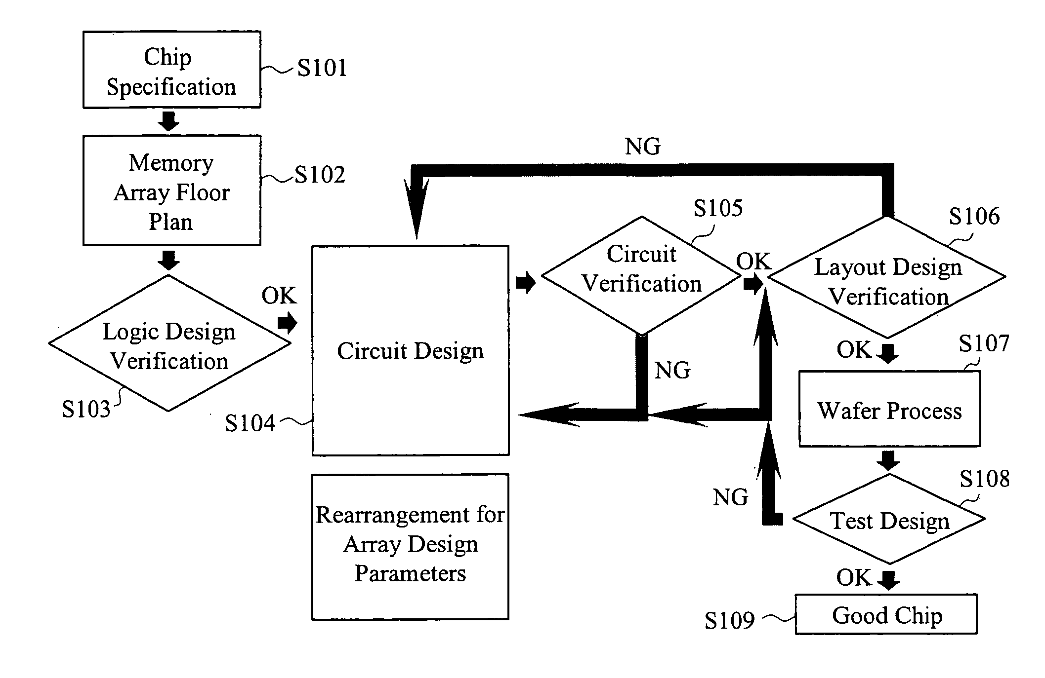
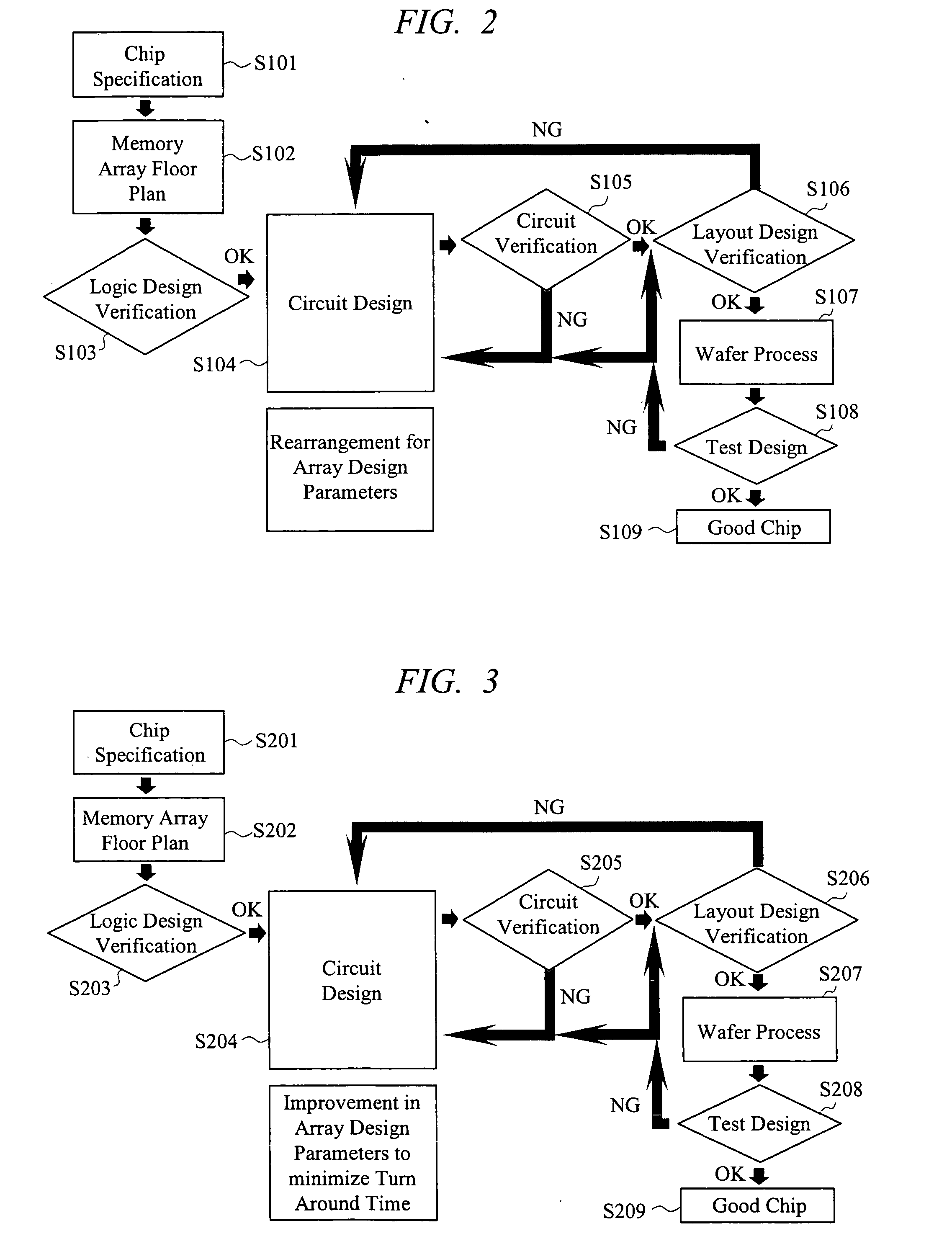
[0053] First, with reference to FIGS. 2 and 3, respective manufacture flows are compared between the case of using the conventional technique and the case of using the present invention. FIG. 2 shows a chip manufacturing flow when the memory array is designed using the conventional worst-case design. FIG. 3 shows a chip manufacturing flow when the design approach according to the present invention is applied to the circuit design.
[0054] As shown in FIG. 2, when the conventional design approach is used, the specification of the chip is established in Step S101. Then, arrangement of circuit blocks in the memory array is determined in Step S102. Next, in Step S103, a logic operation of the memory array is designed with a hardware description language etc., and then is verified. Thereafter, in...
second embodiment
[0097] In the above-mentioned first embodiment, the case of applying the design approach according to the invention to the DRAM design has been described. However, the first embodiment may be applied to a static random access memory (hereinafter referred to as “SRAM”).
[0098]FIGS. 17A and 17B are views for explaining the case of applying the design approach according to the present invention to the SRAM, wherein FIG. 17A shows an example of a circuit diagram of the SRAM and FIG. 17B shows an example of its operating waveform. Reference symbols in the Figure are as follows. That is, “VDD” represents a supply voltage, “ΦLD” a load transistor drive switch, “ΦDR” a driver transistor drive switch, “ΦCSN” and “ΦCSP” common sources, and “I_DL” a H-side readout current, “I_ / DL” an L-side off current, “Vt(I_DL)” a H-side data-line voltage by the read-out current I_DL, and “Vb(I_ / DL)” an L-side data line voltage by the off leakage current I_ / DL. Other reference symbols are similar to those in...
third embodiment
[0103]FIGS. 18A and 18B are views for explaining the case of applying the design approach according to the present invention to a NAND-type non-volatile memory, wherein FIG. 18A is an example of a circuit diagram of the NAND-type non-volatile memory and FIG. 18B is an example of its operating waveform.
[0104] Reference symbols in the Figure are as follows. That is, “ST1” represents a data line connection switch, “CG” a control gate, “FG” a floating gate, “ST2” a source line selection switch, “SL” a source line, “ΦR” a reference power supply drive switch, “VREF” a reference voltage, “IF_DL” a read-out current, and “V(IF_DL)” a data line voltage by the read-out current IF_DL. Since each circuit diagram or driving method for performing the read-out and write-in operation of the memory cell can be realized by using the commonly known circuit diagram or driving method, their detailed descriptions and drawings will be omitted. Additionally, the design approach according to the present inv...
PUM
 Abstract
Description
Claims
Application Information