Poly-crystalline silicon thin film transistor

a thin film transistor and polysilicon technology, applied in the field of polycrystalline silicon thin film transistors, can solve the problems of large leakage current, inability to use in low-temperature polysilicon (ltps) tft, and difficulty in obtaining crystalline grains larger than the size using conventional methods, and achieve the effect of improving interface properties and low leakage curren

Inactive Publication Date: 2006-07-06
SAMSUNG ELECTRONICS CO LTD
View PDF14 Cites 15 Cited by
  • Summary
  • Abstract
  • Description
  • Claims
  • Application Information

AI Technical Summary

Benefits of technology

[0012] The present disclosure provides a polycrystalline silicon thin film...

Problems solved by technology

The maximum size of crystalline grains which can be obtained using such conventional methods is about 3000-4000 Å, and it is difficult to obtain crystalline grains larger than the size using the conventional methods.
The gate insulati...

Method used


Image

  • Poly-crystalline silicon thin film transistor
  • Poly-crystalline silicon thin film transistor
  • Poly-crystalline silicon thin film transistor

Examples


Embodiment Construction

[0020] Hereinafter, embodiments of a poly crystalline silicon thin film transistor (TFT) according to the present invention will be described in detail with reference to the accompanying drawings.

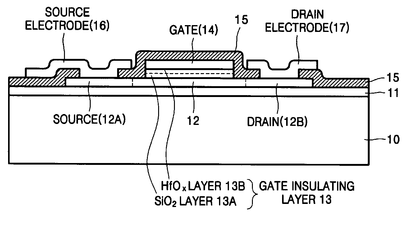
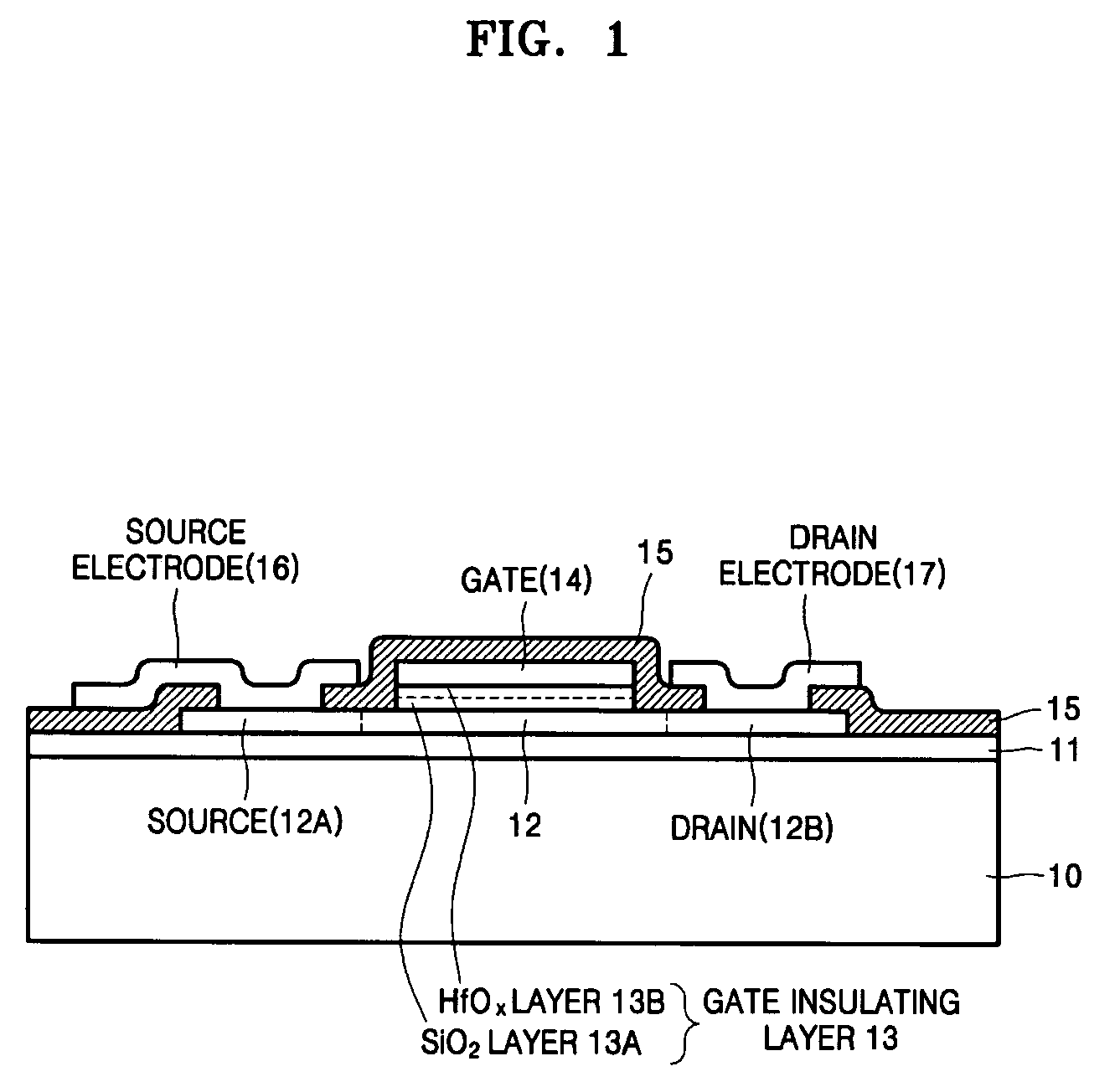
[0021]FIG. 1 is a schematic cross-sectional view of a polycrystalline silicon TFT according to an embodiment of the present invention.

[0022] Referring to FIG. 1, an insulating layer 11 is formed on a substrate 10, which is made of silicon, glass, or plastic, and a silicon channel layer 12 is disposed on the insulating layer 11. A source region 12a and a drain region 12b are formed on both sides of the silicon channel layer 12 by doping. A gate insulating layer 13 is formed on the silicon channel layer 12, and a gate 14 is formed in a center portion of the gate insulating layer 13. An interlayer dielectric (ILD) 15 is formed on the gate 14. The ILD 15 includes openings in regions corresponding to the source region 12a and the drain region 12b. A source electrode 16 is connected to the sour...


PUM

PropertyMeasurementUnit
Thicknessaaaaaaaaaa
Thicknessaaaaaaaaaa
Currentaaaaaaaaaa

Abstract

Provided is a silicon thin film transistor (TFT) including: a substrate; a silicon channel layer formed on the substrate with a source and a drain on both sides thereof; a gate insulating layer formed on the silicon channel layer; and a gate formed on the gate insulating layer, wherein the gate insulating layer has a structure including an HfOx film. The TFT has a low leakage current.

Description

CROSS-REFERENCE TO RELATED PATENT APPLICATIONS [0001] Priority is claimed to Korean Patent Application No. 10-2005-0000381, filed on Jan. 4, 2005, in the Korean Intellectual Property Office, the disclosure of which is incorporated herein in its entirety by reference. BACKGROUND OF THE INVENTION [0002] 1. Field of the Disclosure [0003] The present disclosure relates to a silicon thin film transistor (TFT) having reduced leakage current. [0004] 2. Description of the Related Art [0005] Polycrystalline silicon (poly-Si) has higher mobility than amorphous Si (a-Si), and thus can be applied to flat panel display devices and various electronic devices such as solar batteries. [0006] In general, in order to obtain high quality poly-Si crystalline, a material which is resistant to heat, such as glass, is used. When manufacturing poly-Si crystalline on a heat-resistant material, such as glass, high-temperature a-Si deposition methods, such as chemical vapor deposition (CVD), plasma enhanced C...

Claims


Application Information

Patent Timeline
IPC IPC(8): H01L29/76
CPCH01L29/4908H01L29/66757C08J5/06C08J5/18C08J9/06C08K3/08C08K7/06C08K2003/0812C08K2003/085C08K2003/0856C08L21/00C08L101/00
Inventor NOGUCHI, TAKASHIYIN, HUAXIANGJUNG, JI-SIMXIANYU, WENXUKWON, JANG-YEONROH, YONG-HANJEONG, SUK-WONJEONG, SEONG-HOON
Owner SAMSUNG ELECTRONICS CO LTD
Why Eureka
Try Eureka