Method for producing a silicon-on-insulator structure

a technology of silicon-on-insulator and structure, which is applied in the field of semiconductor/solid-state device manufacturing, electrical equipment, basic electric elements, etc., can solve the problems of low quality of buried oxide in soi structure, high straggling, and reduced production quality of silicon-on-insulator structur

Inactive Publication Date: 2006-07-06
OBSCHESTVO S OGRANICHENNOI
View PDF22 Cites 29 Cited by
  • Summary
  • Abstract
  • Description
  • Claims
  • Application Information

AI Technical Summary

Problems solved by technology

The described above method has a lot of disadvantages that lead to decreasing a quality of produced silicon-on-insulator structures.
Firstly, this is the low quality of buried oxide in SOI structures, which are produced by described method.
Thirdly, the need of using relatively high energy H+ ion implantation due to pass the oxide layer and exfoliate thin silicon layer beneath leads to high straggling in projected range of H+ ions, and properly to the increase in dose needed for exfoliation and defects and hydrogen content in BOX, and to increase in roughness of exfoliated film surface.
Fourthly, it leads to an inhomogeneity in transferring of exfoliated film on the area of first wafer due to starting of exfoliation at few places at the high enough temperature of exfoliation ˜500° and higher.
Fifthly, hydrogen and other gases flatulence in the pores at the bonded interface renders impossible the whole film transfer due to initial adsorbed substances at the surfaces of the bonded wafers with following flaking of transferred film during high temperature treatment in the case of mentioned above method (U.S. Pat. No. 5,374,564), when only one Si layer is transferred on the other substrates.
This known technical solution also has the disadvantages, that diminish the quality of silicon-on-insulator wafers.
Firstly, storage of the pores at the bonded interface due to initial hydrogen accumulation at the pores, created by residual impurities, physically adsorbed at the surfaces of the bonded wafers with following flaking of transferred film due to hydrogen release during high temperature treatment.

Method used


Image

  • Method for producing a silicon-on-insulator structure
  • Method for producing a silicon-on-insulator structure
  • Method for producing a silicon-on-insulator structure

Examples


example 1

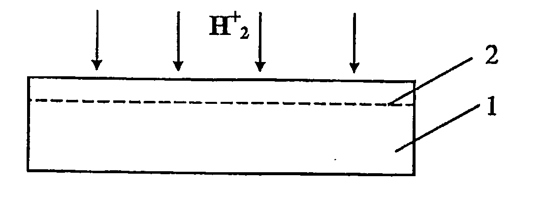
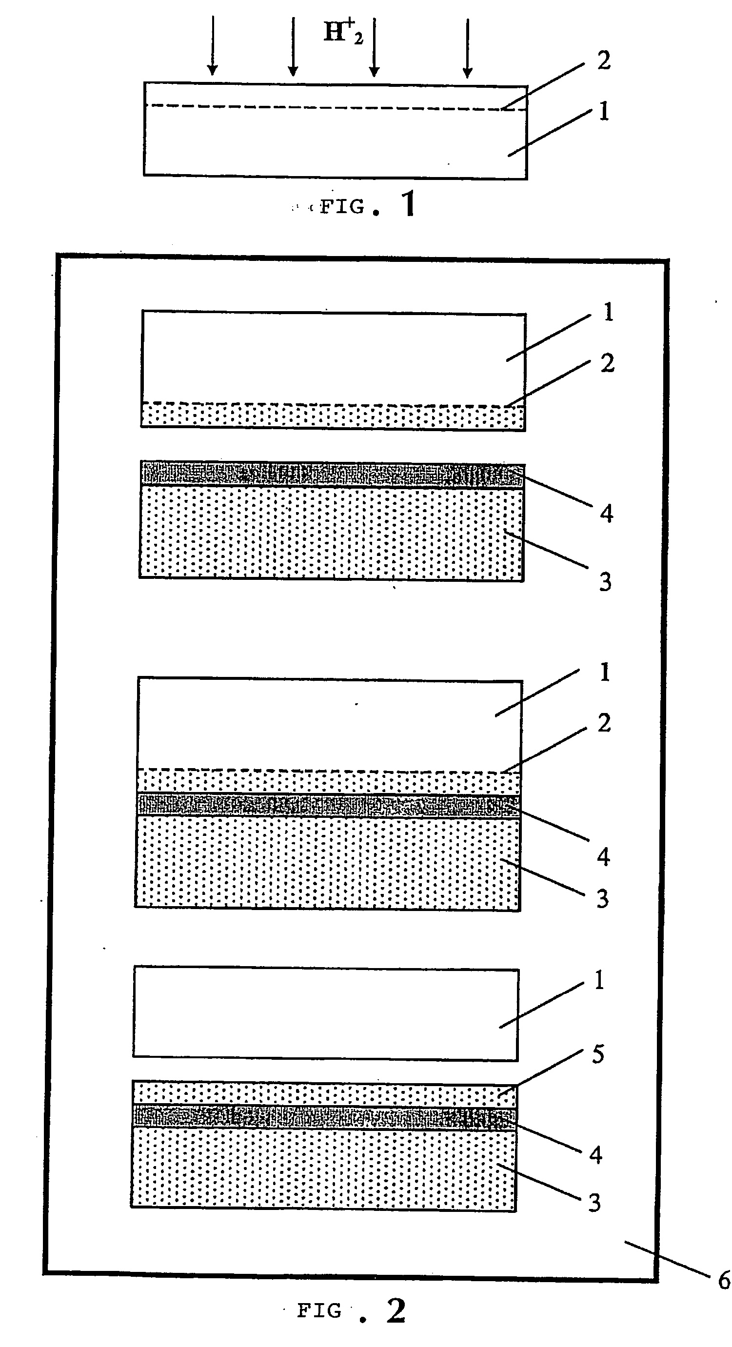
[0044] 1. H2+ ion implantation is carried out in silicon wafer with ion energy 140 keV and dose 2,5×10¹⁶ crm2 through thin 50 nm SiO2 layer, which prevents the surface contamination and following it is removed. [0045] 2. Silicon wafer with grown thermal oxide SiO2 (280 nm) is used as a substrate. [0046] 3. Chemical treatment of implanted silicon wafer and substrate is carried out including cleaning with deionized water stream douche or ultrasonic deionized water stream and hydrophilisation of surfaces of implanted wafer and unimplanted substrate, using treatment in the peroxide-acid and ammonia-peroxide solutions with following cleaning by water stream douche or ultrasonic deionized water stream. [0047] 4. H2+ implanted silicon wafer and silicon wafer with grown thermal oxide are placed in low vacuum chamber with pressure 102 Pa and heated to the temperature 300° C., dried and cleaned from the physically adsorbed substances during 0.1 hour and then joined together, spliced and exfol...

example 2

[0049] 1. H2+ ion implantation is carried out in silicon wafer with ion energy 40 keV and dose 1,5×1016 cm−2 through thin 5 nm SiO2 layer, which prevents the surface contamination and following it is removed. [0050] 2. Silicon wafer with grown thermal oxide SiO2 (280 nm) is used as a substrate. [0051] 3. Chemical treatment of implanted silicon wafer and substrate is carried out including cleaning with deionized water stream douche or ultrasonic deionized water stream and hydrophilisation of surfaces of implanted wafer and unimplanted substrate, using treatment in the RCA and ammonia-peroxide solutions with following cleaning by water stream douche or ultrasonic deionized water stream. [0052] 4. H2+ ion implanted silicon wafer and silicon wafer with grown thermal oxide are placed in low vacuum chamber with pressure 101 Pa and heated to the temperature 200° C., dried and cleaned from the physically adsorbed substances during 0.15 hour, then joined together and heated to 300° C., splic...

example 3

[0054] 1. H2+ ion implantation is carried out in silicon wafer with ion energy 140 keV and dose 5×1016 cm−2 through thin 50 nm SiO2 layer, which prevents the surface contamination and following it is removed. [0055] 2. Silicon wafer with grown thermal oxide SiO2 with the thickness 280 nm is used as a substrate. [0056] 3. Chemical treatment of implanted silicon wafer and substrate is carried out including cleaning with deionized water stream douche or ultrasonic deionized water stream and hydrophilisation of surfaces of implanted wafer and unimplanted substrate, using treatment in the RCA and ammonia-peroxide solutions with following cleaning by water stream douche or ultrasonic deionized water stream. [0057] 4. H2+ ion implanted silicon wafer and silicon wafer with grown thermal oxide are placed in low vacuum chamber with pressure 102 Pa and heated to the temperature 150° C., dried and cleaned from the physically adsorbed substances during 0.2 hour, then joined together and heated t...


PUM

PropertyMeasurementUnit
thicknessaaaaaaaaaa
thicknessaaaaaaaaaa
thicknessaaaaaaaaaa

Abstract

The inventive method for producing a silicon-on insulator structure consists in implanting hydrogen is a silicon plate (1), chemically treating said silicon plate (1) and a substrate (3), in connecting and grafting the silicon plate (1) and the substrate (3) and in layering along the implanted layer (2) of the plate (1). The drying, removal of physically adsorbed substances from the surface of the plate (1) and the substrate (3), connection of the plate (1) and the substrate (3), the grafting and layering thereof along the implanted layer (2) of the plate is carried out after the chemical treatment in one stage, in a low vacuum, at a temperature when hydrogen introduced by implantation remains in a bound state.

Description

FIELD OF THE INVENTION [0001] The invention belongs to semiconductor technology and more exactly deals with the method for producing a silicon-on-insulator (SOI) structure. DESCRIPTION OF THE PRIOR ART [0002] The method for producing a silicon-on-insulator structure is known (U.S. Pat. No. 5,374,564), contained hydrogen implantation in a first wafer, bonding the first wafer with the second wafer and slicing the first wafer. The implantation is realized by ion bombardment of the first wafer with the ions that create a layer, which contains the gas filled micropores in the volume of the first wafers at the depth near the penetration distance of the ions. This layer divides the wafer into the bottom part, that contains the substrate, and the upper part, that contains the thin film. At that hydrogen ions or inert gas ions are used, and the temperature of first wafer is maintained below the temperature, at which the gas created by implanted ions is diffused out of volume of implanted sem...

Claims


Application Information

Patent Timeline
Patent Type & Authority Applications(United States)
IPC IPC(8): H01L21/30H01L21/425H01L21/324H01L21/265H01L21/762
CPCH01L21/26506H01L21/76254
Inventor POPOV, VLADIMIR PAVLOVICHTYSCHENKO, IDA EVGENIEVNA
Owner OBSCHESTVO S OGRANICHENNOI
Why Eureka
Try Eureka