Substrate-processing apparatus and method of producing a semiconductor device
a technology of substrate processing and semiconductor devices, applied in lighting and heating apparatus, charge manipulation, furniture, etc., can solve problems such as temperature limits even on this heating method, and create problems
- Summary
- Abstract
- Description
- Claims
- Application Information
AI Technical Summary
Benefits of technology
Problems solved by technology
Method used
Image

Examples
second embodiment
[0062] the present invention shown in FIG. 4 and FIG. 5 is described next.
[0063] Structural parts in the present embodiment that are equivalent to those in the previous embodiment are assigned the same reference numerals and their description is omitted.
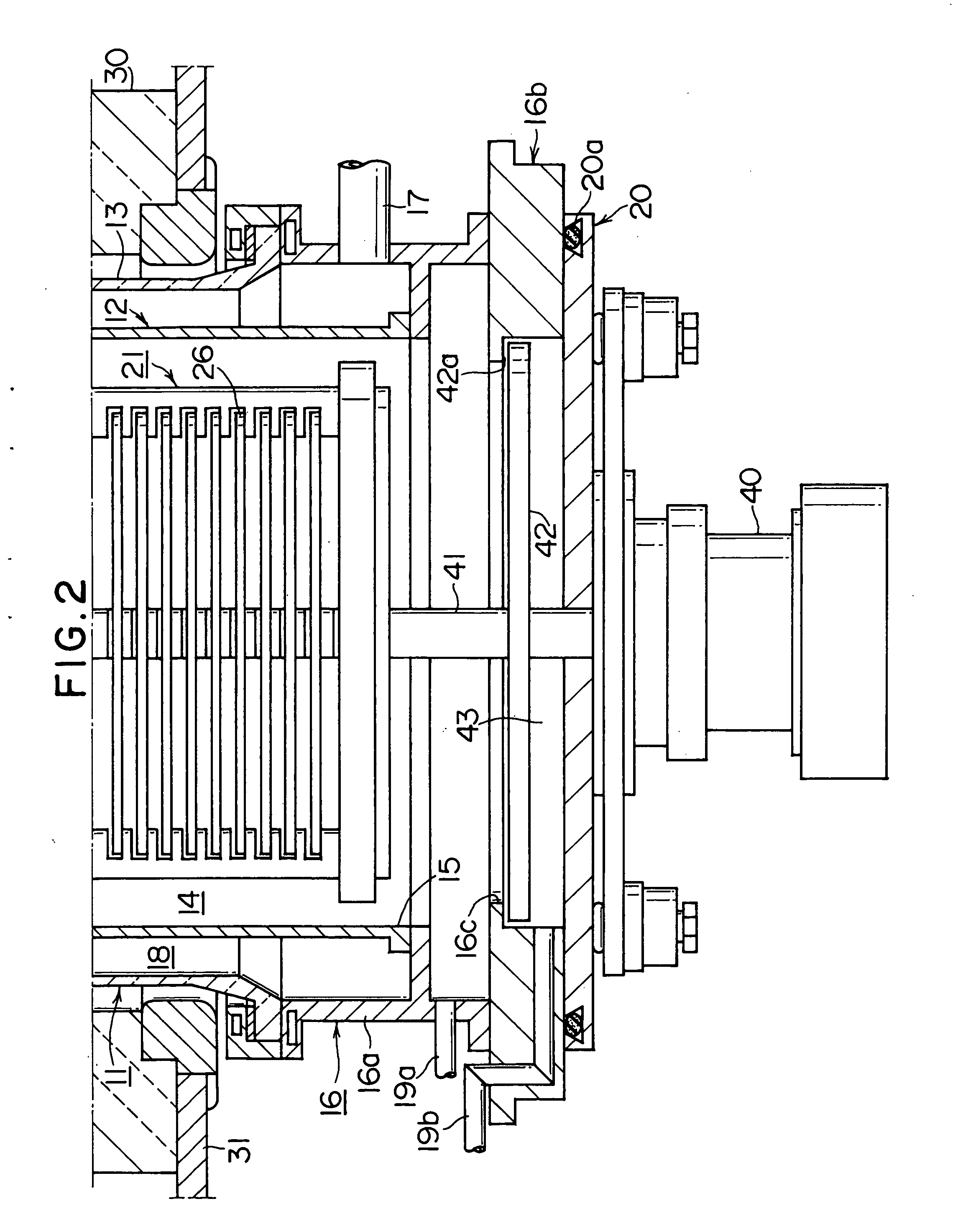
[0064] An upper divider ring section 61 is provided continuously across the entire circumference below an inner tube mount 16d of the furnace opening flange 16. A boat lower flange 62 on the other side, is installed concentrically with a boat mount 49 on the lower surface of the boat mount 49 horizontally supported on the top edge of the rotating shaft 41. The boat lower flange 62 is formed in a ring shape utilizing a high nickel alloy (for example high nickel alloys of 50 percent or more nickel, 15 to 30 percent chromium, and 15 to 30 percent molybdenum) with high corrosion resistance. A lower divider ring section 63 is formed facing the upper divider ring section 61 on the bottom end of the boat lower flange 62. The upper divider ...
third embodiment
[0074] the present invention is described next as shown in FIG. 6 and FIG. 7.
[0075] Structural parts in the present embodiment that are equivalent to those in the previous embodiment are assigned the same reference numerals and their description is omitted.
[0076] A protrusion 12a connecting across the entire circumference is provided on the outer circumferential surface of the bottom end of the inner tube 12. Installing the protrusion 12a on an inner tube mount 16d connecting across the entire circumference on the internal circumference of the furnace opening flange 16, makes the inner tube 12 support on the furnace opening flange 16. An extending section 12b extends below the protrusion 12a of the inner tube 12. A divider ring 27 made from quartz glass or silicon carbide (SiC) is installed as a ring-shaped plate member below the extending section 12b on the seal cap 20. The divider ring 27 is secured to the seal cap 20 by a clamp ring 28. The clearances 29a, 29b of approximately 0...
fourth embodiment
[0088] the present invention is described next while referring to FIG. 8.
[0089] The present embodiment differs from the third embodiment in the point that a gas feed pipe 19c (Hereafter called the third gas feed pipe.) for supplying the third gas G3 to the processing chamber 14 is inserted into the furnace opening flange 16. The gas feed opening of the tip opening (blow vent) of the third gas feed pipe 19c is installed downstream (upwards) of the flow outlet 46a, 46b. Gas supplied from the gas feed opening of the third gas feed pipe 19c mixes downstream of the flow outlets 46a, 46b with the gas flowing from the flow outlets 46a, 46b.
[0090] The third embodiment contains the additional third gas feed pipe 19c and can therefore handle three or more types of gases.
[0091] When using two types of gases, the same gas is preferably supplied from the first gas feed pipe 19b and the second gas feed pipe 19a, while the other gas is supplied from the third gas feed pipe 19c.
[0092] For exampl...
PUM
| Property | Measurement | Unit |
|---|---|---|
| Flow rate | aaaaa | aaaaa |
Abstract
Description
Claims
Application Information
 - R&D
- Intellectual Property
- Life Sciences
- Materials
- Tech Scout
- Unparalleled Data Quality
- Higher Quality Content
- 60% Fewer Hallucinations
Browse by: Latest US Patents, China's latest patents, Technical Efficacy Thesaurus, Application Domain, Technology Topic, Popular Technical Reports.
© 2025 PatSnap. All rights reserved.Legal|Privacy policy|Modern Slavery Act Transparency Statement|Sitemap|About US| Contact US: help@patsnap.com