
Solid state imaging device and production method therefor

a solid-state imaging and production method technology, applied in semiconductor devices, radio-controlled devices, electrical apparatus, etc., can solve the problems of optimum condensing, difficult to obtain the shape of intra-layer condensing lenses that is necessary, and inability to reliably use al that has been used for wiring, etc., to achieve optimum condensing and high precision

Inactive Publication Date: 2006-07-13
SONY CORP
View PDF5 Cites 34 Cited by
  • Summary
  • Abstract
  • Description
  • Claims
  • Application Information

AI Technical Summary

Benefits of technology

[0012] According to a solid-state imaging device of the present invention, in a CMOS-type solid-state imaging device, since an intra-layer lens (concave lens) is formed such that a second layer buries a concave portion formed by etching a first layer with respect to respective light-receiving portions, it is possible to dispose the intra-lens at an appropriate position without depending on the unevenness of the wiring. Accordingly, incident light can be optimally condensed on the light-receiving portion. Being a single intra-lens makes the structure of the intra-lens simplified. In the case where the first wiring and second wiring are formed on both sides of the light-receiving portion, having difference with respect to distance from the light-receiving portion, there is a high possibility that the intra-lens can not be disposed at a required position with respect to the light-receiving portion when the intra-lens is formed and used depending on the unevenness of the wirings. According to the present invention, however, the intra-layer lens (concave lens) can be disposed at a required position without depending on the wirings even in the case of including wirings having difference with respect to distance from the light-receiving portion. In the case where wirings are disposed such that the first wiring and second wiring are integrally formed to be connected to a required voltage source, the intra-layer lens can also be disposed at a required position without being affected by the wirings. Even in a solid-state imaging device in which a gate electrode of a readout transistor is lopsidedly formed with respect to the light-receiving portion, the intra-layer lens can be disposed at a required position without depending on the unevenness of the gate electrode.
[0026] According to the method for manufacturing a solid-state imaging device of the present invention, a concave portion of a first insulation layer is subjected to isotropic etching through a resist mask and later, a second insulation layer is formed to constitute an intra-layer condensing lens. Accordingly, a single intra-layer condensing lens can easily be formed in a CMOS-type solid-state imaging device. Since a high temperature reflow processing is not required, wirings can be formed of metal materials including Al. The shape of the intra-layer condensing lens (the height, position, curvature and the like of lens) can be easily adjusted by changing an opening pattern of a resist mask, etching conditions and the like. Further, only by changing the opening pattern of the resist mask, the center of the intra-layer condensing lens can be biased to the center side of an imaging region from the center of a light-receiving portion. As a result, the pupil correction method using the biased-lens can be adopted as the countermeasure against shading due to oblique light on the periphery of the imaging region. As described above, according to the manufacturing method of the present invention, an intra-layer condensing lens can be formed in the CMOS-type solid-state imaging device with high precision.

Problems solved by technology

Therefore, it is difficult to obtain the shape of the intra-layer condensing lens that is necessary for optimum condensing of light.
In addition, since heat treatment at a high temperature of 800° C. to 950° C. is necessary in the reflow process of the fluid film, it has been impossible to use Al that has been reliably used for wiring.

Method used


Image

  • Solid state imaging device and production method therefor
  • Solid state imaging device and production method therefor
  • Solid state imaging device and production method therefor

Examples


Embodiment Construction

[0044] Hereinafter, an embodiment of the present invention will be explained referring to drawings.

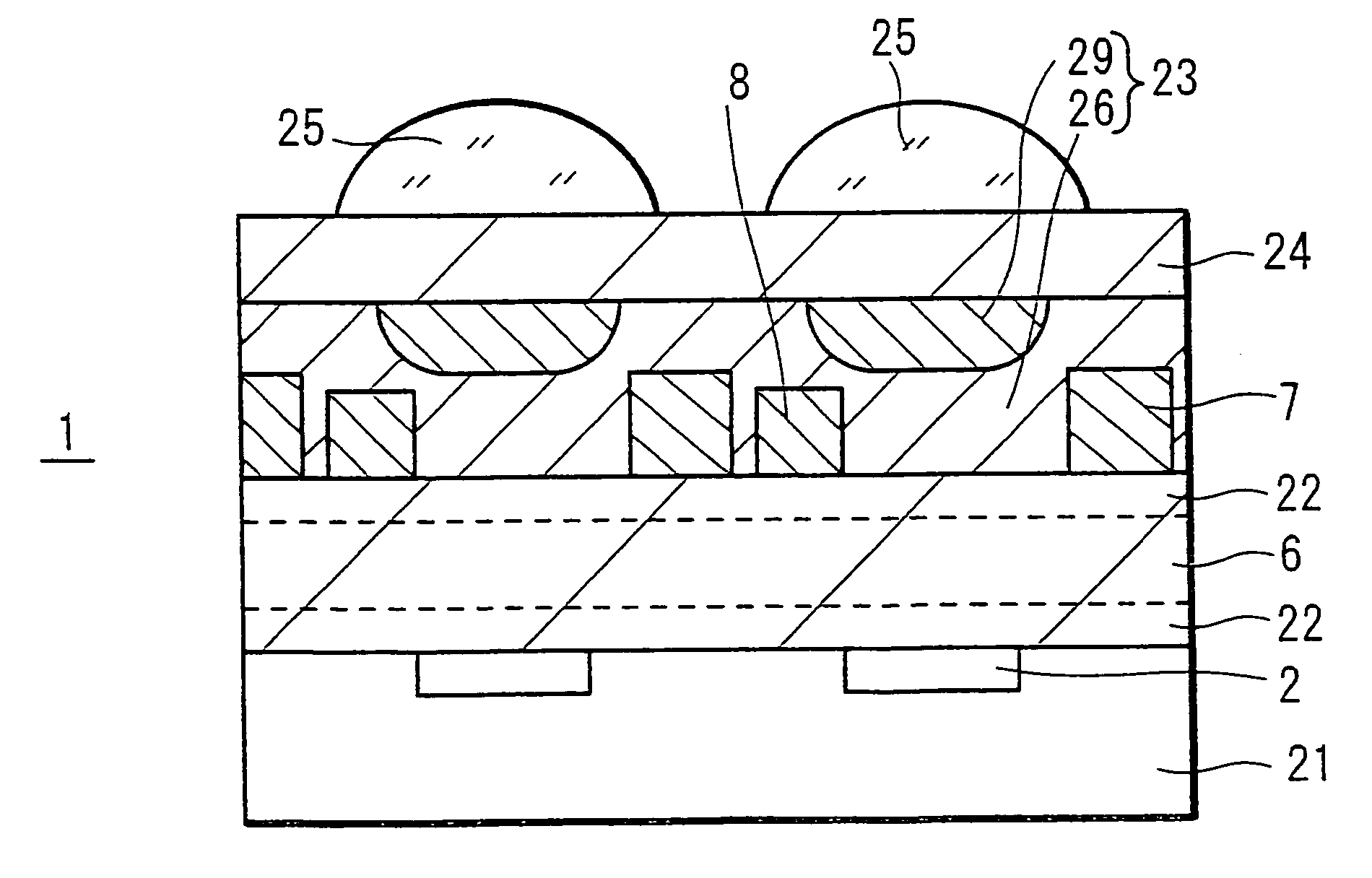
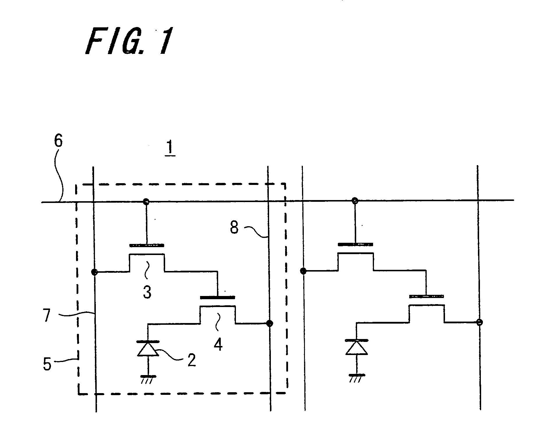
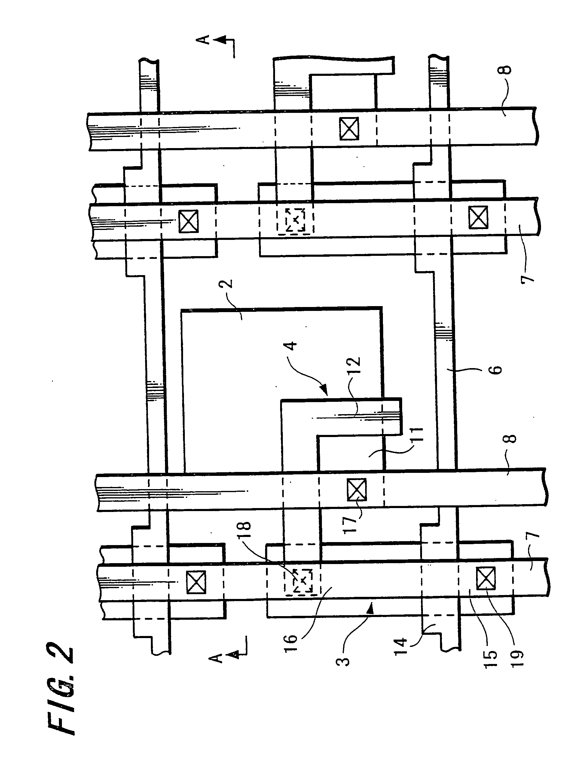
[0045]FIGS. 1 and 2 show the relevant part of an embodiment of a solid-state imaging device according to the present invention, that is, the structure of a pixel portion. The solid-state imaging device according to this embodiment is what is called a CMOS-type solid-state imaging device. As shown in FIG. 1, a solid-state imaging device 1 has an imaging region including a plurality of unit pixels 5 which are disposed in a matrix state and each of which includes a light-receiving portion for conducting photoelectric conversion, that is, a light-receiving sensor portion (namely, photodiode) 2, a vertical selection switch element (MOS transistor) 3 to select a pixel, and a readout switch element (MOS transistor) 4. One main electrode of the readout switch element 4 is connected to the light-receiving sensor portion 2, and a control electrode (what is called a gate electrode) of the readou...


PUM


Abstract

The present invention relates to a CMOS-type solid-state imaging device and a method for manufacturing thereof, and provides a solid-state imaging device capable of optimally condensing light by a single intra-layer lens and a manufacturing method capable of forming an intra-layer lens with high precision. The solid-state imaging device according to the present invention includes a plurality of wirings and a plurality of lenses above a light-receiving portion, in which at least one of the plurality of lenses is formed of a single intra-layer lens. The method for manufacturing the solid-state imaging device according to the present invention includes the processes of forming a concave surface or convex surface onto a first insulation layer with a first refractive index using a selective etching method and forming a second insulation layer with a second refractive index onto the concave surface or convex surface to form the intra-layer lens corresponding to the light-receiving portion.

Description

TECHNICAL FIELD [0001] The present invention relates to a solid-state imaging device including an intra-layer lens and a method for manufacturing thereof. BACKGROUND ART [0002] In a solid-state imaging device, when miniaturization of a light-receiving surface of each sensor portion advances and various kinds of films such as light shielding pattern. and wiring pattern are laminated, an incident light ratio deteriorates. Particularly, in a CMOS-type solid-state imaging device in which a number of light shielding patterns and wiring patterns are laminated, incident light is interrupted by wirings and the like to deteriorate the incident light ratio. As the countermeasure against the deterioration of the incident light ratio, there is known a method in which an intra-layer lens, that is, intra-layer condensing lens is provided between wiring layers corresponding to the upper part of the light-receiving surface to condense light onto a sensor portion without being interrupted by the wir...

Claims


Application Information

Patent Timeline
IPC IPC(8): H01L31/062H01L21/00H01L27/14H01L27/146H01L27/148H01L31/0232H01L31/10
CPCH01L27/14627H01L31/0232H01L27/14685H01L31/02327H01L27/146
Inventor TOUMIYA, YOSHINORI
Owner SONY CORP
Learn More