
Method of removing a low-k layer and method of recycling a wafer using the same

a technology of low-k layer and recycling method, which is applied in the direction of semiconductor/solid-state device manufacturing, basic electric elements, electric apparatus, etc., can solve the problems of parasitic capacitance between the lines, the operation speed of the device is decreased, and the conductive lines may not be well-insulated from each other, so as to improve the manufacturing productivity of semiconductors and low cost

Inactive Publication Date: 2006-07-13
SAMSUNG ELECTRONICS CO LTD
View PDF1 Cites 11 Cited by
  • Summary
  • Abstract
  • Description
  • Claims
  • Application Information

AI Technical Summary

Benefits of technology

[0011] Accordingly, embodiments of the present invention provide a method of removing a low-k layer at a low cost.
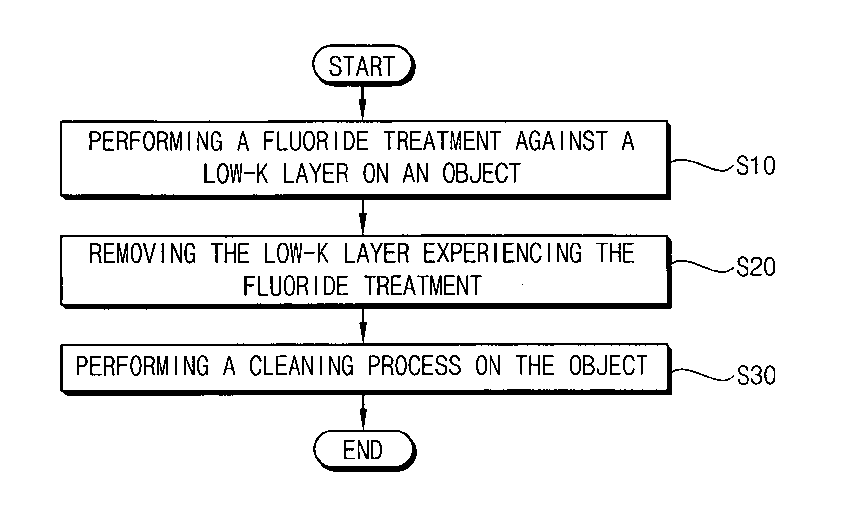
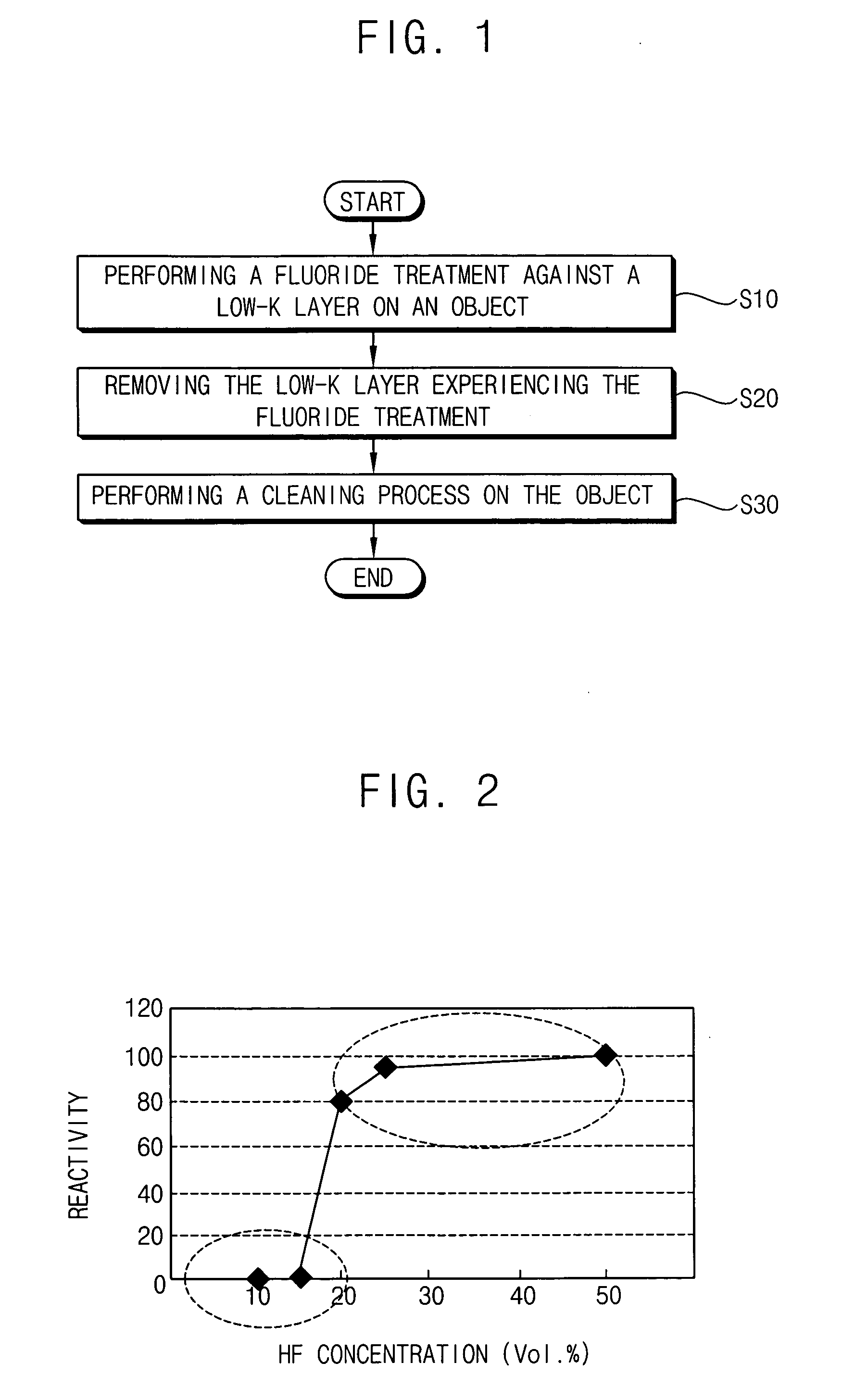
[0015] According to some embodiments of the present invention, a wafer is recycled by removal of a low-k layer from the wafer. The Si—O bond in the low-k layer is broken or is on the verge of breaking the bond due to an aqueous hydrogen fluoride solution, so that the low-k layer is easily removed from the wafer in a subsequent process. Accordingly, the wafer may be recycled at a low cost without any high temperature processes, thereby improving manufacturing productivity of a semiconductor.

Problems solved by technology

As a result, a parasitic capacitance between conductive lines increases and the operation speed of the device is decreased.
However, when the silicon oxide layer is used as an insulation layer for insulating a conductive line in a semiconductor device of which an operation frequency is high and of which a line width is small, conductive lines may not be well-insulated from one another and the parasitic capacitance between the lines necessarily increases.
However, the above removal method has problems in that the hot furnace or plasma is difficult to apply to a mass production and is high cost.

Method used


Image

  • Method of removing a low-k layer and method of recycling a wafer using the same
  • Method of removing a low-k layer and method of recycling a wafer using the same
  • Method of removing a low-k layer and method of recycling a wafer using the same

Examples


Embodiment Construction

[0022] The invention is described more fully hereinafter with reference to the accompanying drawings, in which embodiments of the invention are shown. This invention may, however, be embodied in many different forms and should not be construed as limited to the embodiments set forth herein. Rather, these embodiments are provided so that this disclosure will be thorough and complete, and will fully convey the scope of the invention to those skilled in the art. In the drawings, the size and relative sizes of layers and regions may be exaggerated for clarity.

[0023] It will be understood that when an element or layer is referred to as being “on”, “connected to” or “coupled to” another element or layer, it can be directly on, connected or coupled to the other element or layer or intervening elements or layers may be present. In contrast, when an element is referred to as being “directly on,”“directly connected to” or “directly coupled to” another element or layer, there are no interveni...


PUM


Abstract

In one embodiment, a method of removing a low-k layer at a low cost and a method of recycling a wafer using the same, is described. A fluoride treatment is performed on the low-k layer formed on an object using an aqueous hydrogen fluoride solution, and the low-k layer is removed from the object. The Si—O bond in the low-k layer is broken due to an aqueous hydrogen fluoride solution, so that the low-k layer is easily removed from the wafer. Accordingly, the wafer may be recycled at a low cost, thereby improving manufacturing productivity of a semiconductor.

Description

CROSS REFERENCES TO RELATED APPLICATIONS [0001] This application claims priority from Korean Patent Application No. 2005-2991 filed on Jan. 12, 2005, the content of which is herein incorporated by reference in its entirety. BACKGROUND OF THE INVENTION [0002] 1. Field of the Invention [0003] The present invention relates to a method of removing a low-k layer of which its dielectric constant is very low, and a method of recycling a wafer using the same. More particularly, the present invention relates to a method of removing a low-k layer applicable to a recycle process for a wafer and a method of recycling a wafer using the same. [0004] 2. Description of the Related Art [0005] As information media, such as computers and other electronics, become widely used, the semiconductor industry makes great strides in developing information media products. Functionally, semiconductor devices with a large storage capacity are required to operate at a very high speed. Accordingly, the operation s...

Claims


Application Information

Patent Timeline
Patent Type & Authority Applications(United States)
IPC IPC(8): H01L21/302H01L21/461
CPCH01L21/31053H01L21/31133H01L21/02H01L21/31
Inventor HWANG, DONG-WONLEE, YANG-KOOHEO, DONG-CHULJUN, PIL-KWONLIM, KWANG-SHINLEE, SANG-EON
Owner SAMSUNG ELECTRONICS CO LTD
Learn More