Semiconductor device

Inactive Publication Date: 2006-07-20
HITACHI LTD
View PDF5 Cites 23 Cited by
  • Summary
  • Abstract
  • Description
  • Claims
  • Application Information

AI Technical Summary

Benefits of technology

[0015] When this voltage generator circuit, for example, is used, it becomes possible to fix the terminating resistance of the first transistor by the resistance of the reference resistor. If the reference resistor is a variable resistor, it becomes possible to set a desired terminating resistance adaptively to the characteristics of a transmission line, for example, as explained above. Moreover, because the size of the referential transistor can be reduced to 1/n of the size of the first transistor, the die area occupied by the voltage generator circuit can be reduced.
[0016] If a semiconductor chip has a plurality of signal terminals, it is needed to provide first transistors as described above individually for each signal terminal. However, for example, the gate voltages of these transistors can be controlled in common by using a single voltage generator circuit. Thus, an effect of decreasing the die area by providing an individu

Problems solved by technology

Particularly, in a semiconductor chip having a data transfer speed of several hundred megabits per second to several gigabits per second, reflection waveforms occurring when data is transmitted through the chip become serious.
However, when such a semiconductor chip comes to have an increasing number of s

Method used


Image

  • Semiconductor device
  • Semiconductor device
  • Semiconductor device

Examples


Embodiment Construction

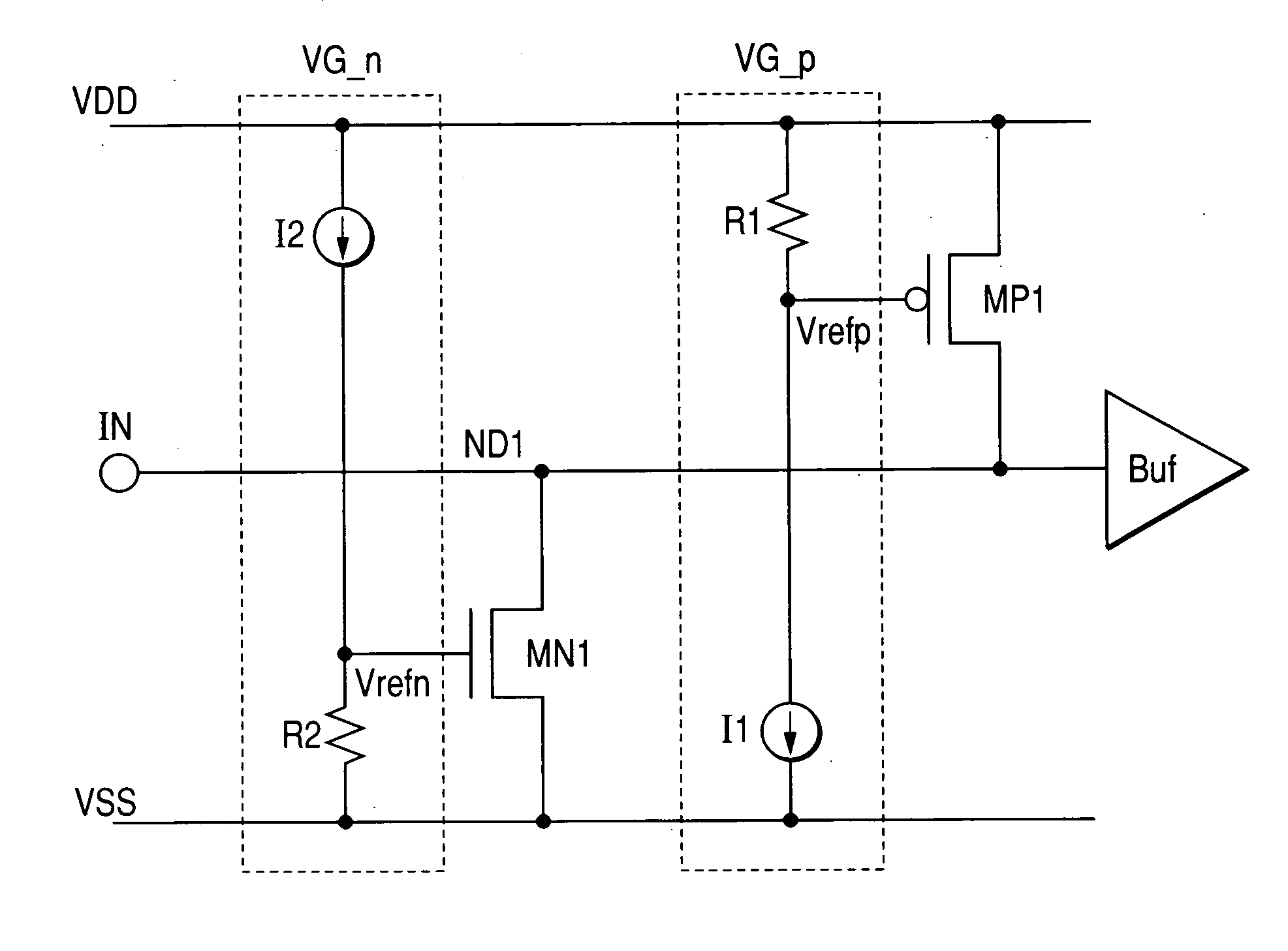
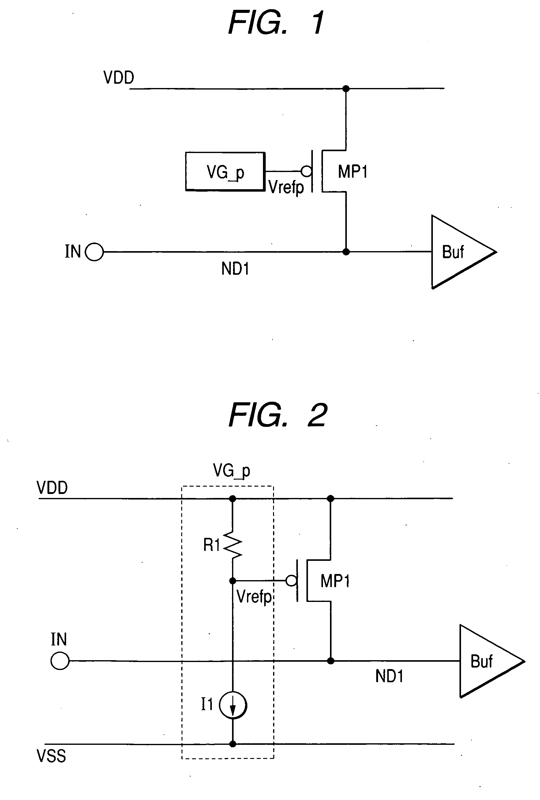
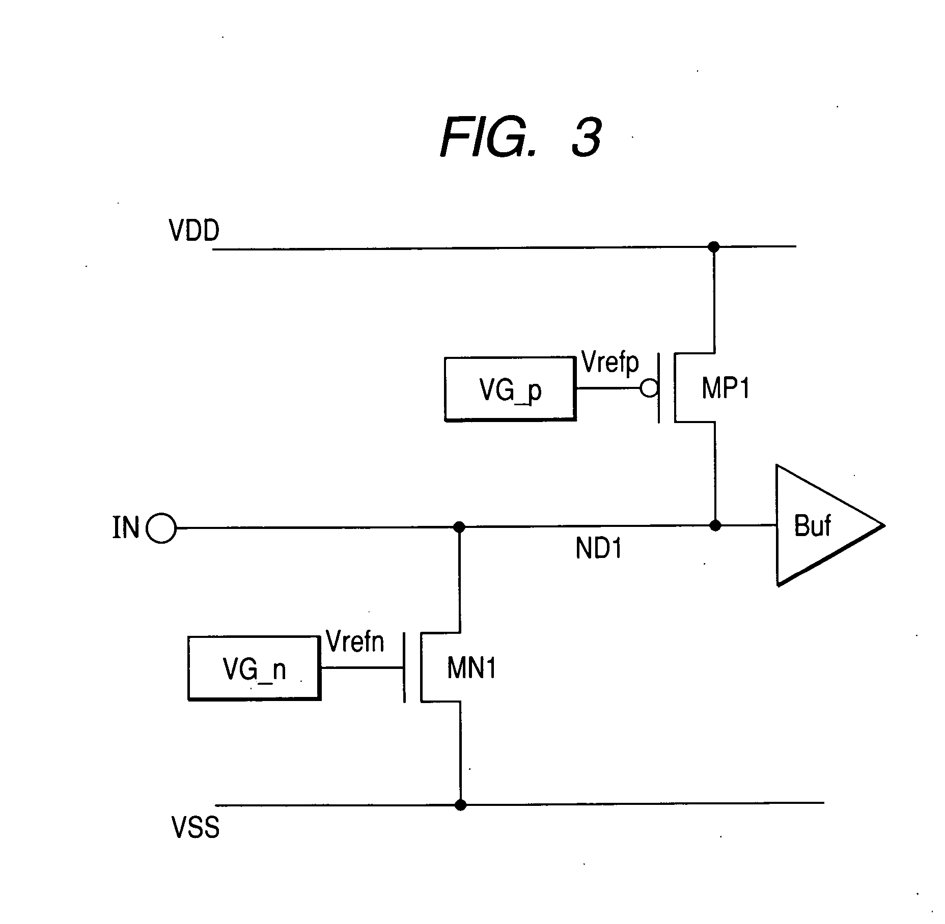
[0032] It is to be understood that the figures and descriptions of the present invention have been simplified to illustrate elements that are relevant for a clear understanding of the present invention, while eliminating, for the purpose of clarity, many other elements found in typical semiconductor devices and methods of making the same. Those of ordinary skill in the art may recognize that other elements and / or steps are desirable and / or required in implementing the present invention. However, because such elements and steps are well known in the art, and because they do not facilitate a better understanding of the present invention, a discussion of such elements and steps is not provided herein. The disclosure herein is directed to all such variations and modifications to such elements and methods known to those skilled in the art.

[0033] Circuit elements constituting each of the functional blocks hereinbelowmay be formed on a monocrystalline silicon semiconductor substrate or th...


PUM


Abstract

This invention provides a semiconductor device in which an ESD protection circuit and a termination circuit can be realized with a small die area. A PMOS transistor having an ESD protection function is placed between a signal node on a line from an signal terminal to an input buffer and a supply voltage node. Furthermore, a voltage generator circuit is placed to supply a reference voltage to the gate of the PMOS transistor. By the reference voltage controlled by the voltage generator circuit, a source-drain resistance of the PMOS transistor is set. Thereby, the PMOS transistor can be made to function as a terminating resistor whose resistance can be set adaptively to a characteristic impedance of a transmission line, for example, connected to the signal terminal in addition to the ESD protection function.

Description

CLAIM OF PRIORITY [0001] The present application claims priority from Japanese application JP 2005-013045 filed on Jan. 20, 2005, the content of which is hereby incorporated by reference into this application. FIELD OF THE INVENTION [0002] The present invention relates to a semiconductor device and more particularly to a technique that is effectively applied to a semiconductor device for high-speed transmission, equipped with an electrostatic discharge (ESD) protection circuit and a signal termination circuit. BACKGROUND OF THE INVENTION [0003] A typical implementation of ESD protection circuit technology is considered below. According to such a circuit, for example, an ESD protection circuit can suppress increases in additional capacitance of a signal terminal is disclosed in JP-A No. 2002-50698. In this circuit construction, a resistor element and a diode-connected (gate-source shorted) PMOS transistor 1 are placed between a signal terminal and a power supply line, a resistor elem...

Claims


Application Information

Patent Timeline
IPC IPC(8): H02H9/00
CPCH01L27/0266H03F1/52
Inventor KAWASHIMO, TATSUYAYAMASHITA, HIROKIYAGYU, MASAYOSHI
Owner HITACHI LTD
Why Eureka
Try Eureka