Innovative growth method to achieve high quality III-nitride layers for wide band gap optoelectronic and electronic devices

Inactive Publication Date: 2006-07-20
LIU XING QUAN +3
View PDF6 Cites 27 Cited by
  • Summary
  • Abstract
  • Description
  • Claims
  • Application Information

AI Technical Summary

Benefits of technology

[0011] A breathing mode epitaxy (BME) approach achieves ultrahigh quality III-nitride epitaxial layers on a low temperature nuclei layer, by supplying the Group V precursors periodically, while keeping the Group III precursor flow constant. In a BME growth mode, AlN epitaxial layers with atomic scale flattened surface have been achieved and the pre-reaction of the precursors was not an issue in the cold wall reactors. The BM

Problems solved by technology

However, a problem exists that the quality of AlxGa1-xN epitaxial layer grown on the HT-AlN template is limited by the quality of the HT-AlN buffer layer.
Even the quality of the AlN/AlxGa1-xN superlattice is limited by the quality of the AlN layers.
However, this continuous epitaxy approach results in HT-AlN epitaxial layers that have a rougher surface than when other known approaches are used.
However, the PALE approach has too low a growth rate for mass production, and too frequent valve acti

Method used


Image

  • Innovative growth method to achieve high quality III-nitride layers for wide band gap optoelectronic and electronic devices
  • Innovative growth method to achieve high quality III-nitride layers for wide band gap optoelectronic and electronic devices
  • Innovative growth method to achieve high quality III-nitride layers for wide band gap optoelectronic and electronic devices

Examples


Embodiment Construction

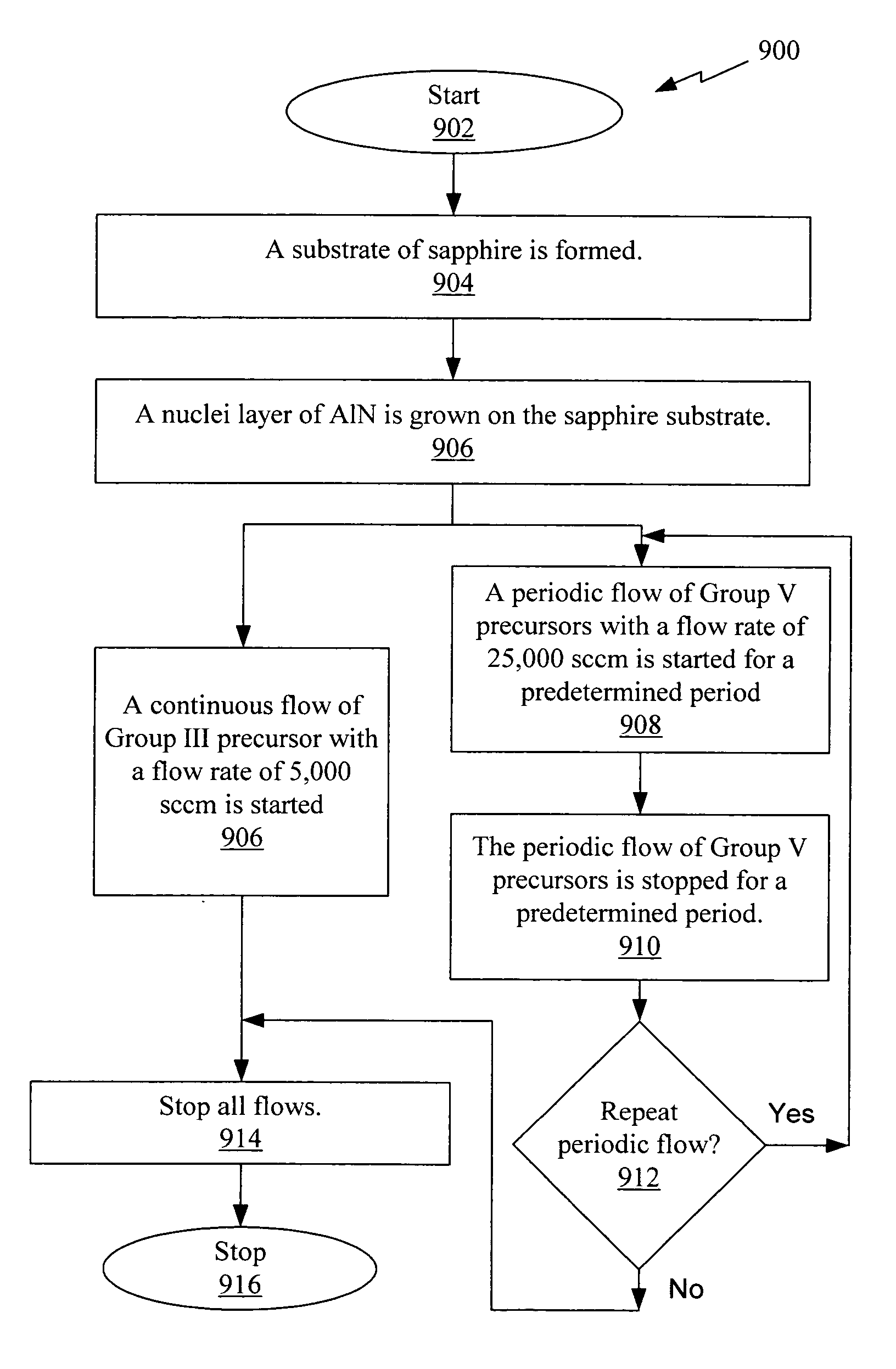
[0023] In the following description of the preferred implementation, reference is made to the accompanying drawings that form a part hereof, and in which is shown by way of illustration a specific implementation in which the invention may be practiced. It is to be understood that other implementations may be utilized and structural changes may be made without departing from the scope of the present invention.

[0024] The present implementation has an epitaxy of atomic scale flattened HT-AlN epitaxial layer on a LT-AlN nuclei layer. Compared with those based on conventional grown HT-AlN buffer layers, high quality AlxGa1-xN epitaxial layers and much improved UV light emitters (UVLEDs) based on BME-grown HT-AlN on sapphire have been demonstrated.

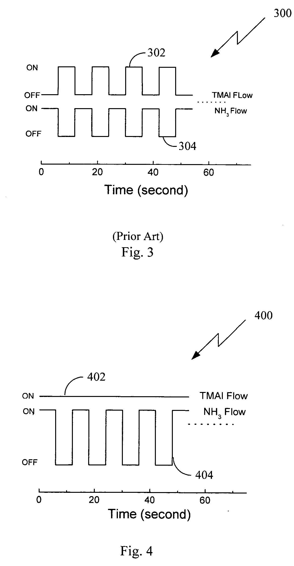
[0025] In FIG. 4, a precursor flow chart of the BME growth in accordance with an implementation is shown. An LT-AlN nuclei layer (20˜100 nm) is grown on sapphire substrate at a low temperature range (500˜650 C.) by continuous growth. After the...


PUM


Abstract

A method to achieve high quality III-nitride epitaxial layers including AlN, AlGaN, GaN, InGaN, and AlInGaN, by supplying group III precursors constantly and group V precursors periodically with the epitaxial growth systems including metal organic chemical vapor deposition (MOCVD), hydride vapor phase epitaxy (HVPE), and molecular beam epitaxy (MBE).

Description

BACKGROUND OF THE INVENTION [0001] 1. Field of Invention [0002] The invention relates to a method of making high quality electronic and optoelectronic device structures, and more particularly to III-nitride electronic and optoelectronic devices. [0003] 2. Related Art [0004] There is a growing worldwide demand for ultraviolet (UV) light emitting diodes (LEDs). The UV LEDs are typically used in such applications as biochemical media detection, white light sources, and UV detection to name but a few. High quality UV LEDs may be manufactured using wide band gap III-nitride material approaches such as AlxGa1-xN on GaN, AlN, SiC substrates. Some known approaches also have used sapphire substrates with mixed results. [0005] Some of the approaches that are known in the art use AlxGa1-xN on sapphire substrates, such as AlN / AlxGa1-xN superlattice and high temperature AlN (HT-AlN) on sapphire substrates. The HT-AlN layer acts as a buffer and strain-releasing layer. However, a problem exists th...

Claims


Application Information

Patent Timeline
IPC IPC(8): H01L29/22H01L21/28H01L31/0296
CPCH01L21/0242H01L21/02458H01L21/02513H01L21/0254H01L21/0262H01L33/007
Inventor LIU, XING-QUANXIN, HUOPINGSONG, JIN JOOCHOO, THOMAS K.
Owner LIU XING QUAN
Why Eureka
Try Eureka