Dual PCI-X/PCI-E card

a technology of printed circuit board and bus interface, which is applied in the direction of programmable/customizable/modifiable circuits, electrical apparatus construction details, instruments, etc., can solve the problems of limiting the number of peripherals that can be efficiently supported by a system, the theoretical limit of conventional pci bus technology is very close to its practical limit, and minor performance gains are possible. , to achieve the effect of reducing the fabrication cost of the chipset and simplifying the fabrication process

Active Publication Date: 2006-07-20
AVAGO TECH INT SALES PTE LTD
View PDF12 Cites 10 Cited by
  • Summary
  • Abstract
  • Description
  • Claims
  • Application Information

AI Technical Summary

Benefits of technology

[0013] The present invention is directed to a PCB having multiple different bus interface connectors, and a chipset that supports the multiple bus interfaces. In an embodiment, the present invention includes a dual PCI-X / PCI-E interface PCB. As a result, the dual interface functionality of a PCI-X / PCI-E chipset can be fully taken advantage of by the user, operating the chipset on either a PCI-X or a PCI-E bus. Furthermore, chipset fabrication costs can be reduced as well as the fabrication process simplified, by the production of a single dual bus interface PCB instead of multiple board variations to support various bus interface types.

Problems solved by technology

However, with the exponential growth of CPU power, bus technology based on the conventional PCI architecture is becoming more and more a bottleneck to enhanced system performance.
The main reason for that being that a shared bus technology suffers from a scalability problem, limiting the number of peripherals that can be efficiently supported by a system.
At its current state, the conventional PCI bus technology is theoretically very close to its practical limits, with only minor performance gains possible at large costs in form factor.
Although PCI-E clearly provides major performance improvements compared to the conventional PCI standard and its extensions (parallel PCI), serial PCI-E is not backward compatible with parallel PCI, and the shift from parallel PCI to PCI-E is likely to be a slow one.
As a result, dual bus chipsets have to be mounted on multiple PCB variations to support the various bus interface types, denying the user the interface duality of the chipset component, and running higher fabrication costs to chipset manufacturers.
This solution is clearly a costly and inefficient one from a fabrication process point of view.

Method used


Image

  • Dual PCI-X/PCI-E card
  • Dual PCI-X/PCI-E card
  • Dual PCI-X/PCI-E card

Examples


Embodiment Construction

Overview

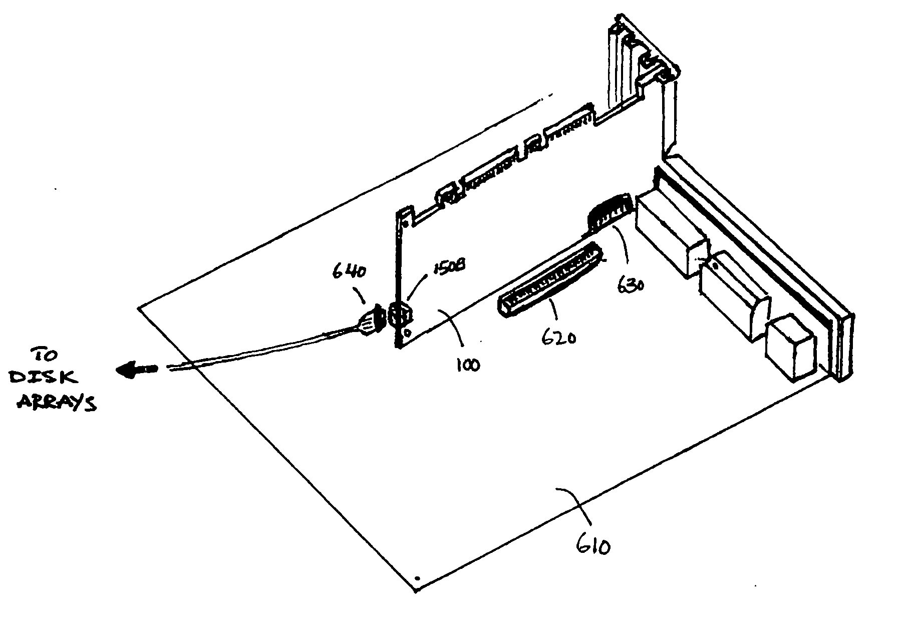
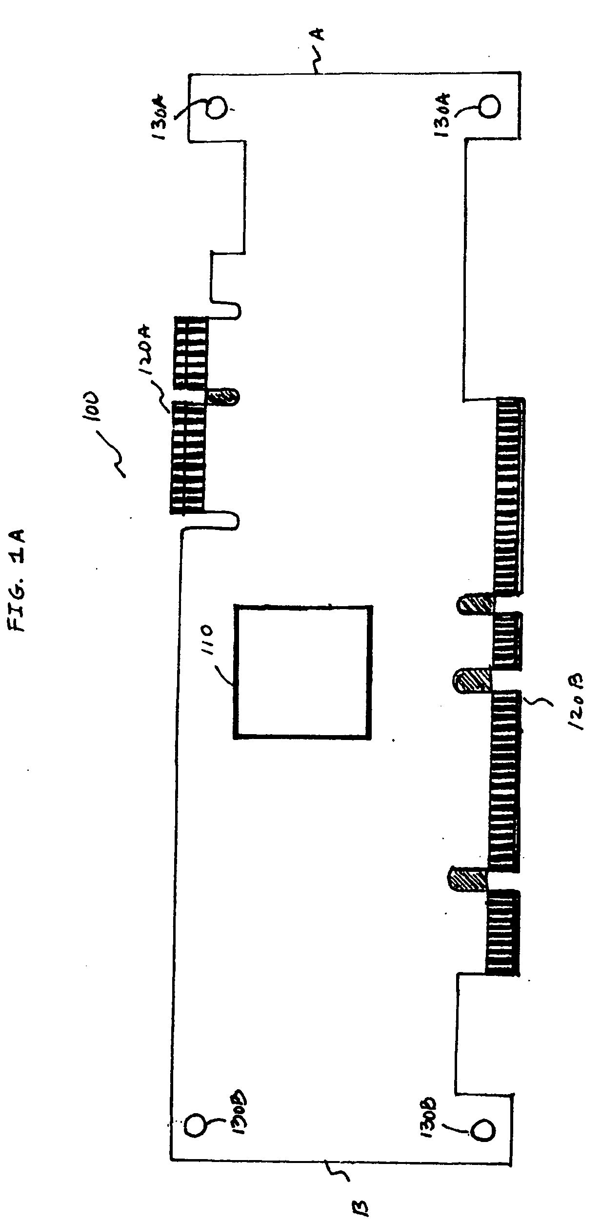
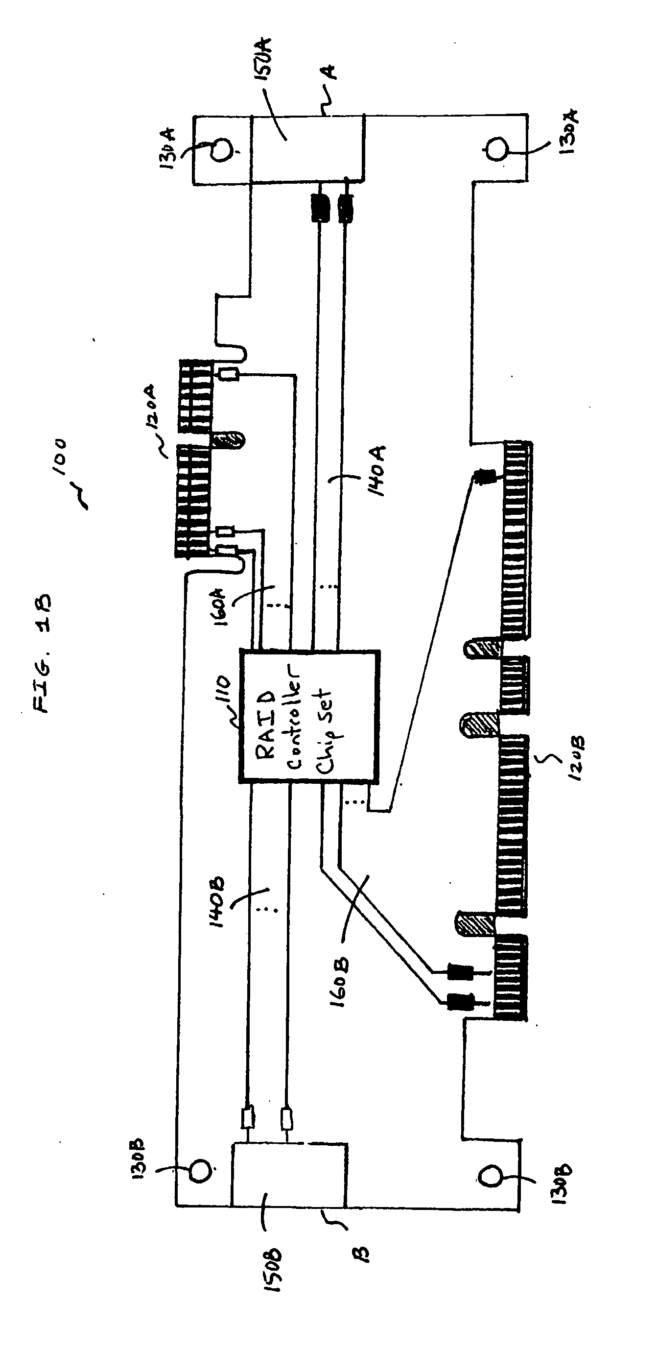
[0028]FIG. 1A shows a top view of an example dual-interface PCB 100 according to the present invention. In the example, the PCB 100 includes a main chipset 110, a first interface connector 120A, a second interface connector 120B, and two pairs of screw holes 130A and 130B located on edges A and B of the PCB 100, respectively. The main chipset 110 is an electronic chipset that supports two different types of bus interfaces. The two pairs of screw holes 130A and 130B allow the PCB 100 to be attached to a computer case from either edge A or edge B. Other attachment mechanisms can also be employed.

[0029] In the example of FIG. 1A, the interface connectors 120A and 120B are illustrated at opposite edges of the PCB 100. The invention is not, however, limited to this example. Based on the description herein, one skilled in the relevant art(s) will understand that connectors 120A and 120B can be positioned on adjacent edges or on the same edge of PCB 100.

[0030] In another exampl...


PUM


Abstract

A dual bus interface PCB includes a main chipset component, a first type bus interface connector, and a second type bus interface connector. The PCB can be configured at fabrication time to enable a variety of configurations for operation. Optionally, the PCB can also be provided at least one memory chip and a NIC (Network Interface Card) chip. By virtue of having a dual interface, the PCB can be used with either the first type or the second type bus. Furthermore, the dual interface PCB eliminates the need by chipset manufacturers to carry multiple PCB variations of the same product in order to support various bus interfaces. In one embodiment, the PCB is a dual PCI-X/PCI-E interface PCB.

Description

BACKGROUND OF THE INVENTION [0001] 1. Field of the Invention [0002] The invention herein relates in general to a dual bus interface printed circuit board (PCB) and more particularly to a PCB provided with both a PCI-X (Peripheral Component Interconnect-Extended) bus interface and a PCI-E (Peripheral Component Interconnect-Express) bus interface. [0003] 2. Background Art [0004] In the field of I / O Interconnect, PCI (Peripheral Component Interconnect) is a widely adopted I / O bus standard in a wide variety of computer platforms. To meet the growing demand for bandwidth by new applications, PCI has gone through several changes in the last decade leading to extension standards such as PCI-2.2 and PCI-X (PCI-Extended). These extension standards however are all built on the same architecture, protocols, signals, and connector as the conventional PCI, the reuse having been mainly supported by the combination of backward compatibility and the ease of migration from the conventional PCI to th...

Claims


Application Information

Patent Timeline
Patent Type & Authority Applications(United States)
IPC IPC(8): G06F13/36
CPCH05K1/0295H05K1/117H05K1/181H05K2201/09954
Inventor PURWIN, CHARLES J.
Owner AVAGO TECH INT SALES PTE LTD
Why Eureka
Try Eureka