High electron mobility devices

Inactive Publication Date: 2006-07-27
KUZMIK JAN
View PDF82 Cites 37 Cited by
  • Summary
  • Abstract
  • Description
  • Claims
  • Application Information

AI Technical Summary

Benefits of technology

[0022] According to yet another aspect, a HEMT (or HFETs) is used a communications system comprising: (a) fabricating the hetero-interface field effect transistor using the steps of: providing a substrate; and fabricating a layered QW structure including at least a barrier layer and a channel layer wherein barrier layer includes InxAl1-xN where 0≦x≦0.30; and (b) using the fabricated hetero-interface field effect transistor in the communications system.
[0023] According to yet another aspect, a HEMT (or HFETs) is used in an electronic device comprising an electronic circuit including a hetero-interface field effect transistor using having a substrate; and a layered quantum well structure including at least a barrier layer and a channel layer providing a polarization-induced charge.
[0024] In general, an electronic device utilizing a hetero-interface field effect transistor include

Problems solved by technology

However, the impurities cause the electrons (or holes) to slow down because they alte

Method used


Image

  • High electron mobility devices
  • High electron mobility devices
  • High electron mobility devices

Examples


Embodiment Construction

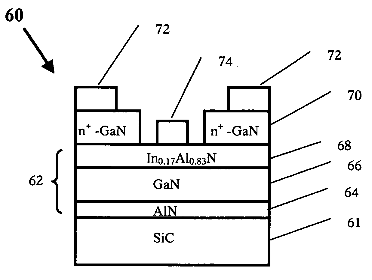
[0039]FIG. 3 illustrates a HEMT 60 according to a first preferred embodiment. HEMT 60 includes a substrate 61, a quantum well (QW) structure 62 and electrodes 72 and 74. Preferably, quantum well structure 62 includes an AlN buffer layer 64, an un-doped GaN layer 66, and an un-doped InAlN layer 68. A doped n+-GaN layer 70 is used to form ohmic contacts with source and drain electrodes 72.

[0040] HEMT 60 is a III-nitride HEMT fabricated on a (0001) 6H—SiC substrate 61 using molecular-beam epitaxy (MBE) or metal-organic vapor phase epitaxy (MOVPE). AlN buffer layer 64 has a thickness in the range of 10 nm to 40 nm and preferably about 20 nm. GaN layer 66 has a thickness in the range of 1 μm to 3 μm and preferably about 2 μm and the carrier concentration preferably less than about 1×1016 cm−3. An un-doped In0.17Al0.83N barrier layer 68 has a thickness in the range of about 5 nm to 30 nm, and preferably about 15 nm. The highly doped n+ GaN cap layer 70 has a thickness in the range of abo...


PUM


Abstract

The present invention is directed to high frequency, high power or low noise devices such as low noise amplifiers, amplifiers operating at frequencies in the range of 1 GHz up to 400 GHz, radars, portable phones, satellite broadcasting or communication systems, or other devices and systems that use high electron mobility transistors, also called hetero-structure field-effect transistors. A high electron mobility transistor (HEMT) includes a substrate, a quantum well structure and electrodes. The high electron mobility transistor has a polarization-induced charge of high density. Preferably, the quantum well structure includes an AlN buffer layer, an un-doped GaN layer, and an un-doped InAlN layer.

Description

[0001] This application is a continuation of U.S. application Ser. No. 10 / 772,673, filed on Feb. 5, 2004, which is a continuation of PCT Application PCT / SK02 / 00018, filed Jul. 15, 2002, which claims priority from U.S. Provisional Application 60 / 310,546 filed Aug. 7, 2001.1. FIELD OF THE INVENTION [0002] The present invention relates to high electron mobility transistors (HEMTs), also called hetero-structure field-effect transistors (HFETs), having polarization-induced charge of high density. 2. DESCRIPTION OF THE RELATED ART [0003] High electron mobility transistors (HEMT) are field effect devices that use high mobility carriers. Most conventional semiconductor devices use semiconductor layers doped with n-type impurities to generate electrons (or p-type impurities to generate holes) as carriers. However, the impurities cause the electrons (or holes) to slow down because they alter periodicity of the lattice structure, i.e., they form defects that cause collisions. On the other hand...

Claims


Application Information

Patent Timeline
IPC IPC(8): H01L33/00H01L29/20H01L29/778
CPCH01L29/2003H01L29/7786
Inventor KUZMIK, JAN
Owner KUZMIK JAN
Why Eureka
Try Eureka