Gallium nitride-based light emitting device having light emitting diode for protecting electrostatic discharge, and melthod for manufacturing the same

Inactive Publication Date: 2006-07-27
SAMSUNG ELECTRO MECHANICS CO LTD
View PDF4 Cites 86 Cited by
  • Summary
  • Abstract
  • Description
  • Claims
  • Application Information

AI Technical Summary

Benefits of technology

[0022] According to the present invention, two GaN-based LEDs (that is, the main GaN-based LED and the ESD protecting GaN-based LED) are separately formed on a single substrate, thereby allowing the GaN-based light emitting device having an enhanced resistance to reverse ESD to be more easily manufactured. In the present invention, an additional electrode forming process is not required to form Schottky contact. Moreover, since the existin

Problems solved by technology

Although the gallium nitride-based light emitting device has a significant energy band gap, it is generally vulnerable to ESD.
As such, the gallium nitride-based light emitting device is more vulnerable to the reverse ESD than the forward ESD.
Thus, when a large reverse ESD voltage is applied in a pulse shape to the gallium nitride-based light emitting device, the light emitting device can be damaged.
Such a reverse ESD damages reliability of the gallium nitride-based light emitting device as well as causing a sharp reduction in life span thereof.
However, in this method, an additional Zener diode must

Method used


Image

  • Gallium nitride-based light emitting device having light emitting diode for protecting electrostatic discharge, and melthod for manufacturing the same
  • Gallium nitride-based light emitting device having light emitting diode for protecting electrostatic discharge, and melthod for manufacturing the same
  • Gallium nitride-based light emitting device having light emitting diode for protecting electrostatic discharge, and melthod for manufacturing the same

Examples


example

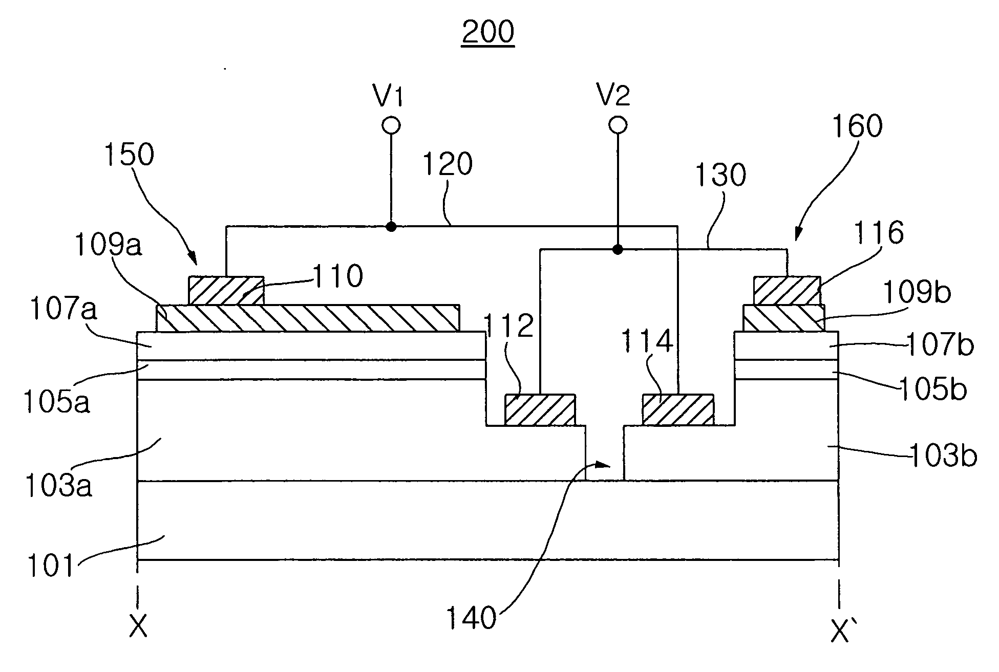
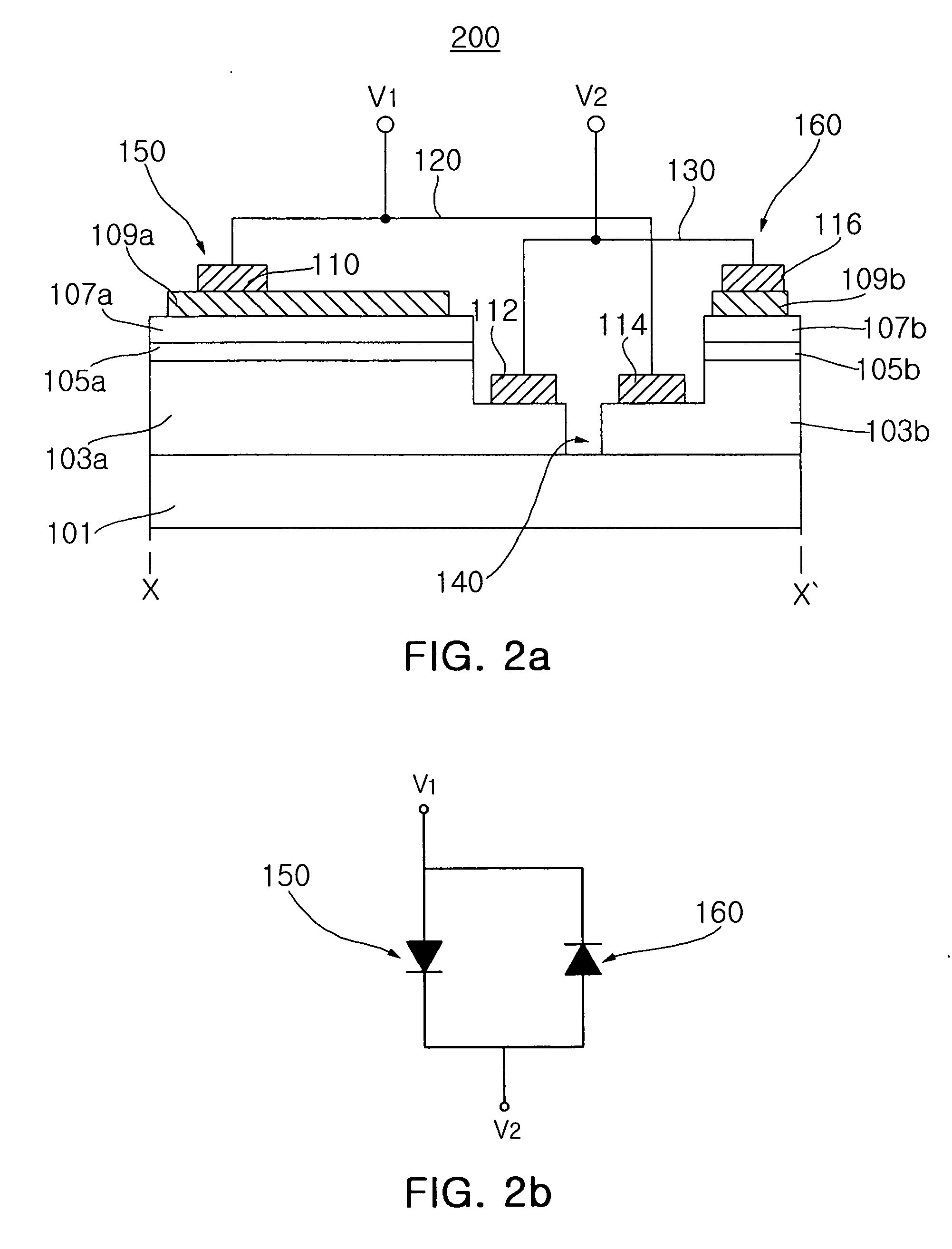
[0047] In order to verify ESD characteristics of a gallium nitride-based light emitting device according to the invention, tests were conducted for detecting breakdown voltages against forward and reverse ESD. In these tests, the gallium nitride light emitting device of the inventive example includes a main LED having a size of 610 μm×200 μm, and an ESD protecting LED connected in parallel to the main LED and having a size of 100 μm×200 μm. Cr / Au metal layers are used for n-side and p-side electrodes, and an ITO layer is used for transparent layers. On the contrary, the GaN-based light emitting device of the conventional example does not have the ESD protecting LED, and comprises one GaN-based LED. The GaN-based LED of the conventional GaN-based light emitting device has the same size as that of the GaN-based light emitting device of the invention.

[0048] As results of detecting the ESD characteristics of the GaN-based light emitting devices of the inventive and conventional example...


PUM


Abstract

A gallium nitride-based light emitting device, and a method for manufacturing the same are provided. The light emitting device comprises a substrate; a main GaN-based LED including a first p-side electrode and a first n-side electrode, the main GaN-based LED formed in a first region on the substrate; and an ESD protecting GaN-based LED including a second p-side electrode and a second n-side electrode, the ESD protecting GaN-based LED formed in a second region on the substrate. The first region is separated from the second region by a device isolation region. The first p-side and n-side electrodes are electrically connected to the second n-side and p-side electrodes, respectively.

Description

RELATED APPLICATION [0001] The present invention is based on, and claims priority from, Korean Application Number 2005-7587, filed Jan. 27, 2005, the disclosure of which is incorporated by reference herein in its entirety. BACKGROUND OF THE INVENTION [0002] 1. Field of the Invention [0003] The present invention generally relates to a gallium nitride-based light emitting device and a method for manufacturing the same, and, more particularly, to a gallium nitride-based light emitting device, designed to have an enhanced resistance to reverse electrostatic discharge (ESD), and a method for manufacturing the same. [0004] 2. Description of the Related Art [0005] Generally, a conventional gallium nitride-based light emitting device comprises a buffer layer, an n-type GaN-based clad layer, an active layer, and a p-type GaN-based clad layer sequentially stacked on a dielectric sapphire substrate. Additionally, a transparent electrode and a p-side electrode are sequentially formed on the p-t...

Claims


Application Information

Patent Timeline
IPC IPC(8): H01L21/00H01L33/00H01L33/08H01L33/32H01L33/42
CPCH01L27/15H01L33/32B43K23/008B44C5/02
Inventor SHIN, HYOUN SOOKIM, HYUN KYUNGPYEON, IN JOONKIM, CHANG WAN
Owner SAMSUNG ELECTRO MECHANICS CO LTD
Why Eureka
Try Eureka