Semiconductor device and method for fabricating the same

Inactive Publication Date: 2006-07-27
PANASONIC CORP
View PDF2 Cites 6 Cited by
  • Summary
  • Abstract
  • Description
  • Claims
  • Application Information

AI Technical Summary

Benefits of technology

[0034] According to this invention, the capacitor upper electrode is electrically connected to the semiconductor substrate even during the fabrication of the semiconductor device, and therefore, charge stored in the upper electrode can be prevented from flowing to the semiconductor substrate through the capacitor dielectric film. Accordingly, since the process damage of the capacitor dielectric film caused after forming the upper electrode can be reduced, the degrada

Problems solved by technology

The aforementioned conventional semiconductor device and the fabrication method for the same have, however, the following problem:
As a result, the tantalum oxide fi

Method used


Image

  • Semiconductor device and method for fabricating the same
  • Semiconductor device and method for fabricating the same
  • Semiconductor device and method for fabricating the same

Examples


embodiment 1

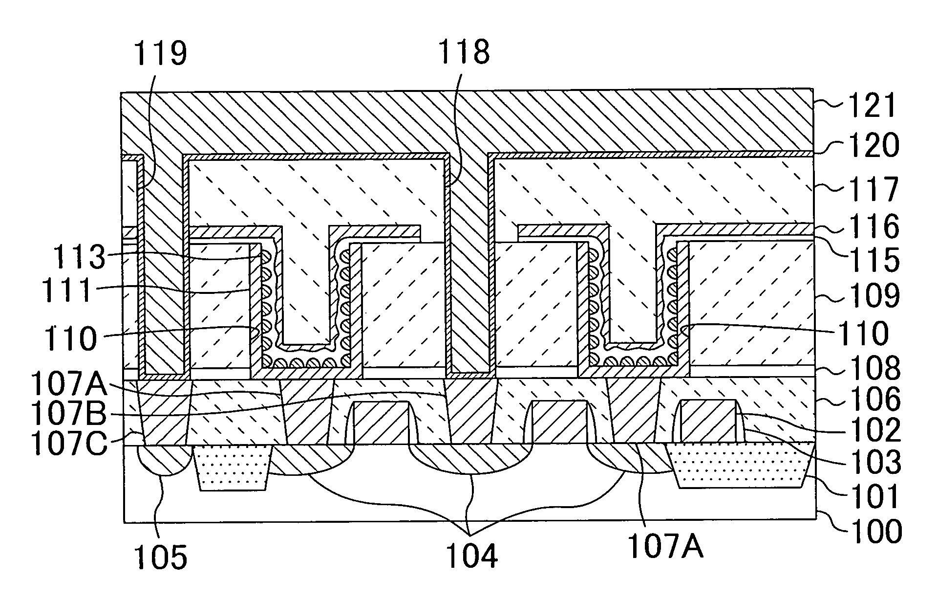
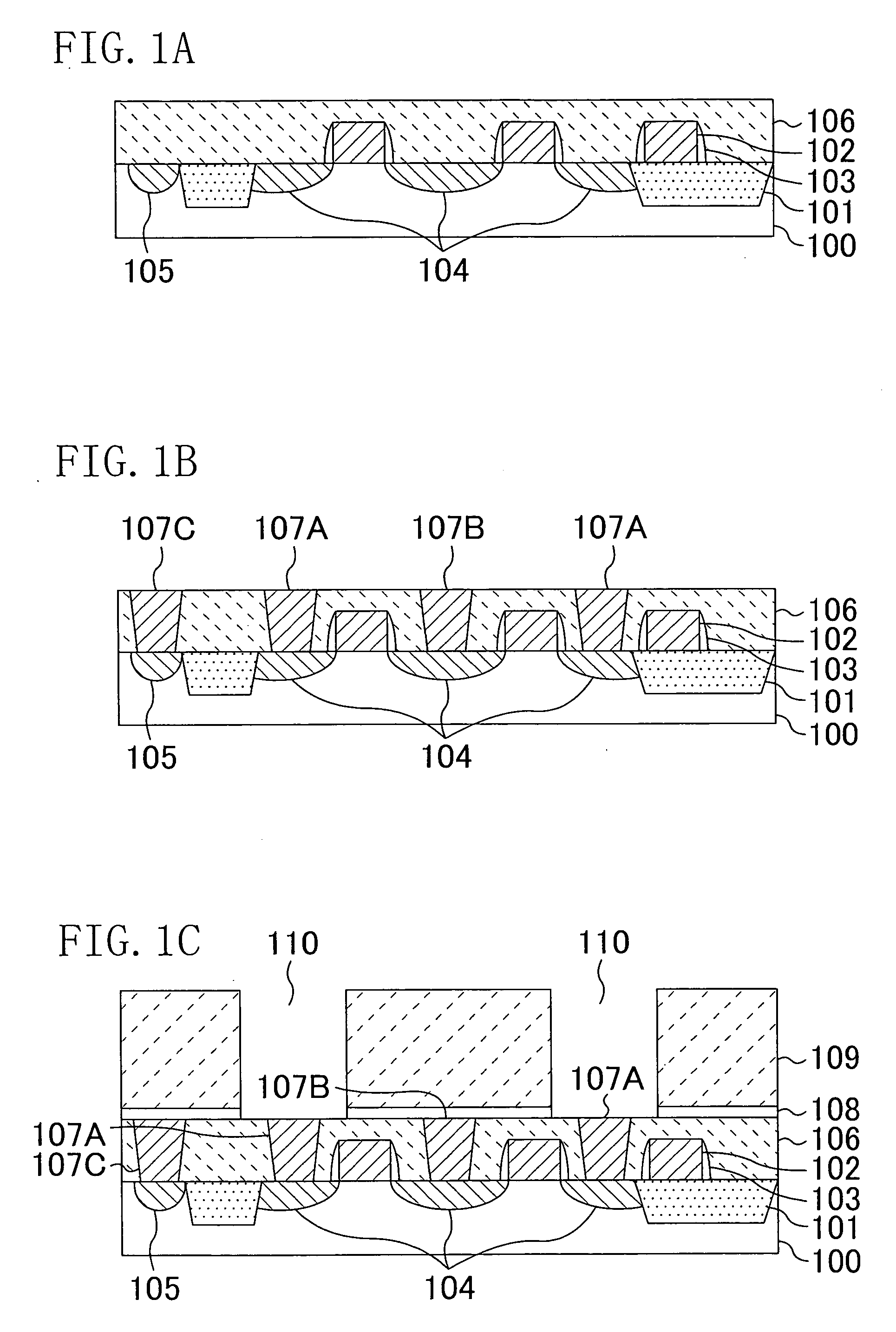
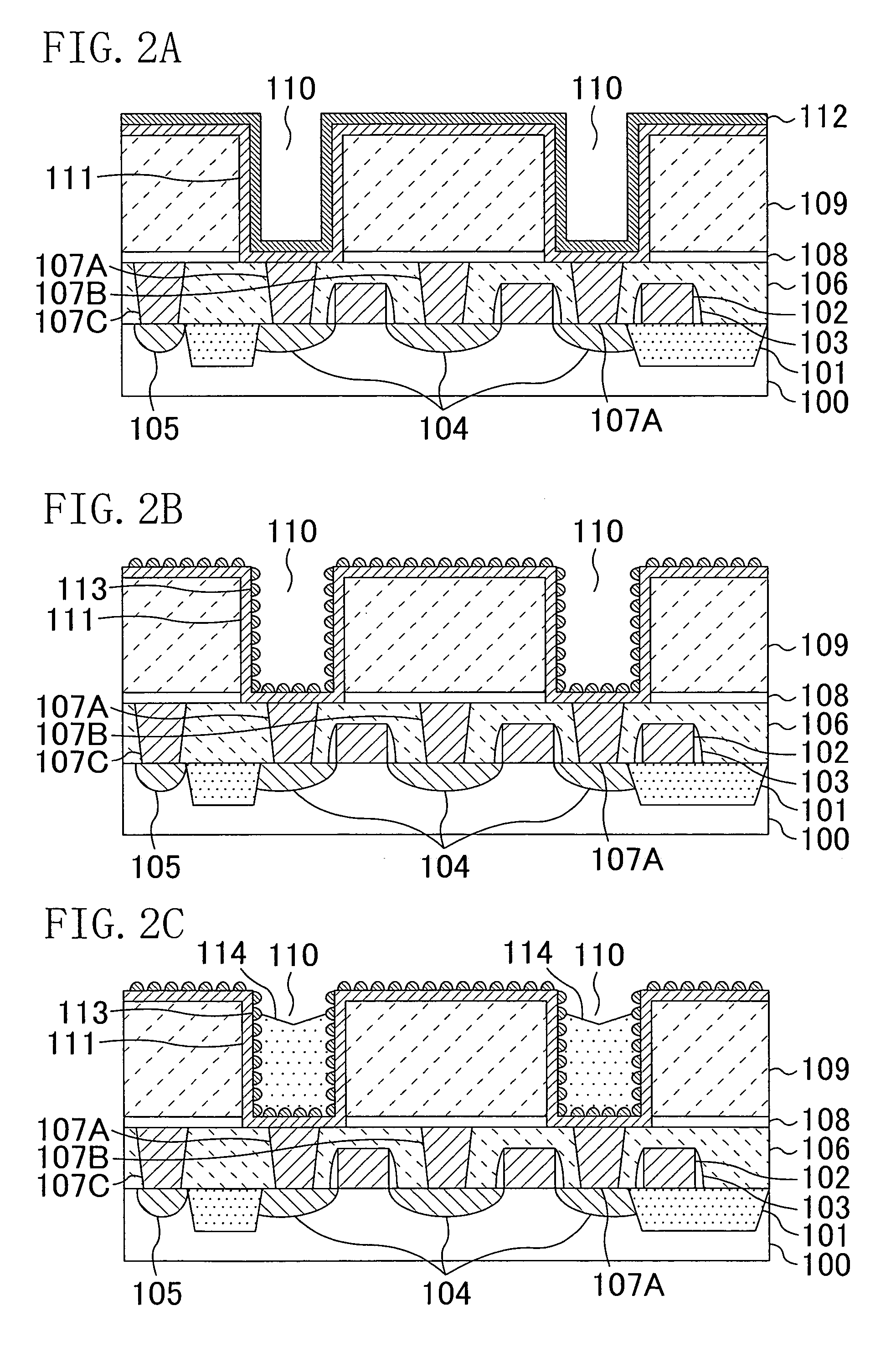
[0061] Now, a semiconductor device and a method for fabricating the semiconductor device according to Embodiment 1 of the invention will be described with reference to the accompanying drawings.

[0062]FIGS. 1A through 1C, 2A through 2C, 3A through 3C, 4A, 4B, 5A and 5B are cross-sectional views for showing procedures in the method for fabricating the semiconductor device of Embodiment 1.

[0063] First, as shown in FIG. 1A, after forming a shallow trench isolation region 101 in a semiconductor substrate 100 of, for example, silicon, a p-type impurity such as boron (B) is implanted into the semiconductor substrate 100 at energy of 15 keV and a dose of approximately 8×10¹² / cm2 for controlling a threshold voltage of a DRAM cell transistor. Next, a gate insulating film (not shown) with a thickness of, for example, 7.5 nm and a first polysilicon film with a thickness of, for example, 200 nm are successively deposited on the semiconductor substrate 100, and then, the first polysilicon film ...

embodiment 2

[0087] Now, a semiconductor device and a fabrication method for the semiconductor device according to Embodiment 2 of the invention will be described.

[0088]FIGS. 7A through 7C, 8A through 8C, 9A through 9C, 10A, 10B, 11A and 11B are cross-sectional views for showing procedures in the method for fabricating the semiconductor device of Embodiment 2.

[0089] First, as shown in FIG. 7A, after forming a shallow trench isolation region 201 in a semiconductor substrate 200 of, for example, silicon, a p-type impurity such as boron (B) is implanted into the semiconductor substrate 200 at energy of 15 keV and a dose of approximately 8×10¹² / cm2 for controlling a threshold voltage of a DRAM cell transistor. Next, a gate insulating film (not shown) with a thickness of, for example, 7.5 nm and a first polysilicon film with a thickness of, for example, 200 nm are successively deposited on the semiconductor substrate 200, and then, the first polysilicon film is patterned by the lithography and the ...

embodiment 3

[0110] Now, a semiconductor device and a fabrication method for the semiconductor device according to Embodiment 3 of the invention will be described.

[0111]FIGS. 12A through 12C, 13A through 13C, 14A, 14B and 15A through 15C are cross-sectional views for showing procedures in the method for fabricating the semiconductor device of Embodiment 3.

[0112] First, as shown in FIG. 12A, after forming a shallow trench isolation region 301 in a semiconductor substrate 300 of, for example, silicon, a p-type impurity such as boron (B) is implanted into the semiconductor substrate 300 at energy of 15 keV and a dose of approximately 8×10¹² / cm2 for controlling a threshold voltage of a DRAM cell transistor. Next, a gate insulating film (not shown) with a thickness of, for example, 7.5 nm and a first polysilicon film with a thickness of, for example, 200 nm are successively deposited on the semiconductor substrate 300, and then, the first polysilicon film is patterned by the lithography and the dry...


PUM


Abstract

A semiconductor device includes a first insulating film formed on a semiconductor substrate; a second insulating film formed on the first insulating film and having a recess corresponding to a capacitor region; a lower electrode formed in the recess; a capacitor dielectric film formed on the lower electrode; and an upper electrode formed on the capacitor dielectric film. The semiconductor device further includes a conductive portion formed in the first insulating film and the second insulating film for electrically connecting the semiconductor substrate to the upper electrode.

Description

CROSS-REFERENCE TO RELATED APPLICATIONS [0001] This application claims priority under 35 U.S.C. §119 on Patent Application No. 2005-015579 filed in Japan on Jan. 25, 2005, the entire contents of which are hereby incorporated by reference.BACKGROUND OF THE INVENTION [0002] The present invention relates to a semiconductor device and a method for fabricating the same, and more particularly, it relates to a semiconductor device including a stack type capacitor and a method for fabricating the same. [0003] Recently, there are demands that a semiconductor device such as a DRAM (dynamic random access memory) should have a smaller memory cell area for attaining refinement and a high degree of integration and have larger capacitance per unit area of a memory cell capacitor. In order to meet the demands, a variety of capacitor structures have been proposed. In particular, in a stack type capacitor, it is easy to increase an opposing area between electrodes of the capacitor owing to its struct...

Claims


Application Information

Patent Timeline
IPC IPC(8): H01L29/00H01L21/44H01L21/8242H01L27/108
CPCH01L21/76816H01L27/10811H01L27/10882H01L27/10894H01L28/84H10B12/312H10B12/48H10B12/09
Inventor ITO, SATORU
Owner PANASONIC CORP
Why Eureka
Try Eureka