Electron beam apparatus

a technology of electron beam and beam tube, which is applied in the direction of discharge tube luminescnet screen, non-electron-emitting shielding screen, etc., can solve the problem that the electron-emitting device is destroyed by discharge and becomes apt to happen, and achieves high reliability

Inactive Publication Date: 2006-07-27
CANON KK
View PDF24 Cites 22 Cited by
  • Summary
  • Abstract
  • Description
  • Claims
  • Application Information

AI Technical Summary

Benefits of technology

[0014] An object of the present invention to provide an electron beam apparatus that prevents surface creeping discharge newly arising due to discharge arising between an anode electrode and an electron-emitting device and is highly reliable. Moreover, another object is to provide the electron beam apparatus without adding cumbersome manufacturing process.

Problems solved by technology

However, the inter-substrate distance gets shorter, then the electric field between the substrates gets high and therefore such a phenomenon that an electron-emitting device is destroyed by discharge becomes apt to take place.
The configuration disclosed in Japanese Patent Application Laid-Open No. 2003-157757 only controls the direction of flow of discharge current and will not prevent surface creeping discharge itself.

Method used


Image

  • Electron beam apparatus
  • Electron beam apparatus
  • Electron beam apparatus

Examples


example 1

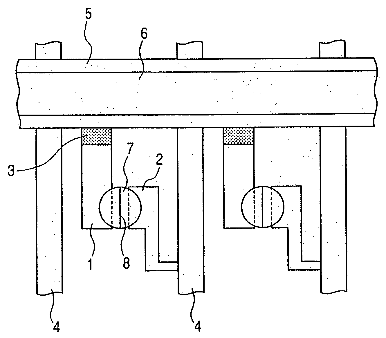
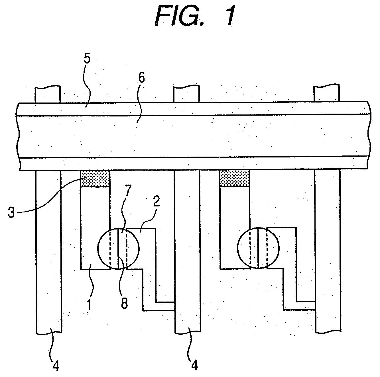
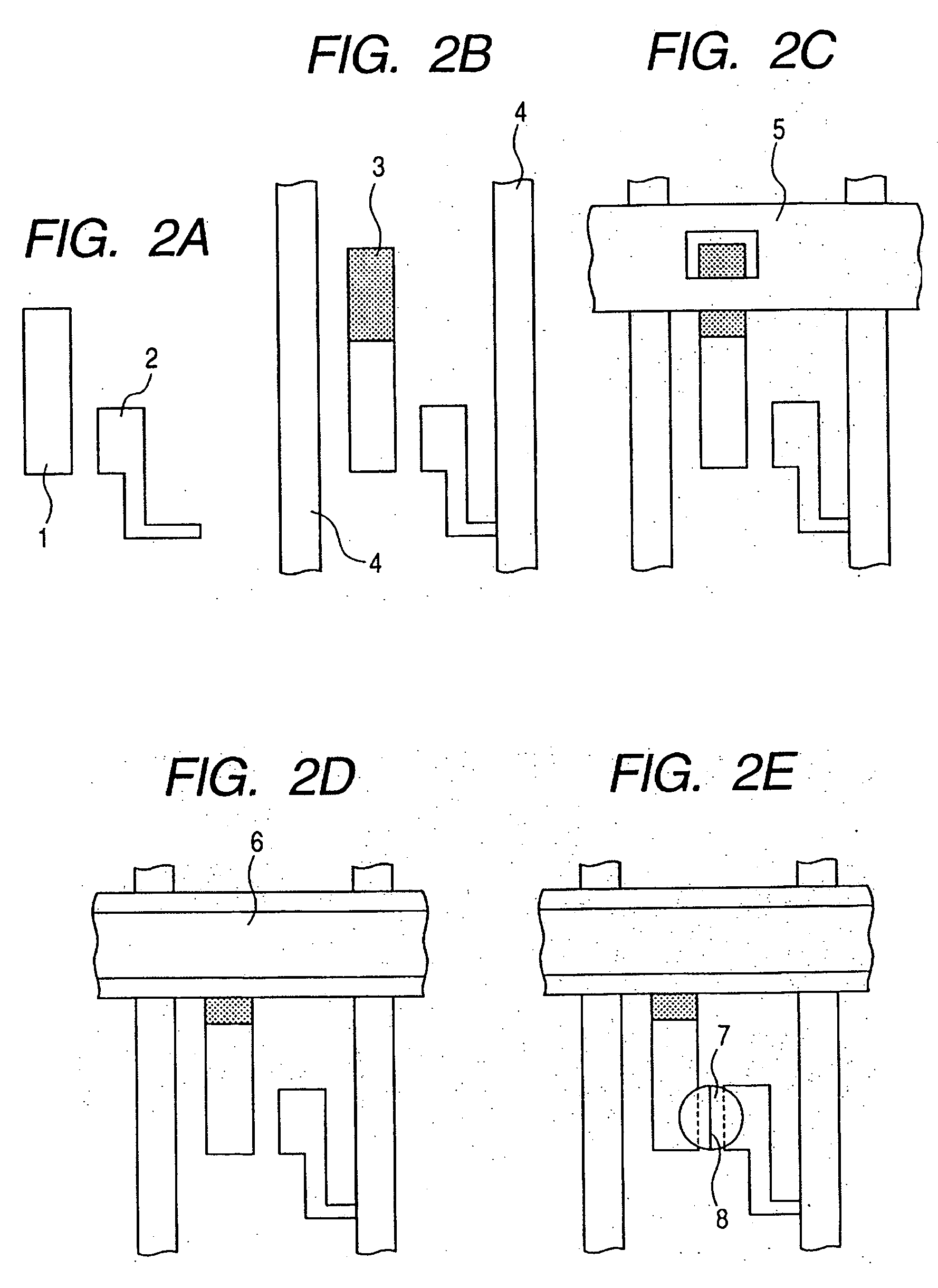
[0115] A rear plate configured as shown in FIG. 1 has been produced in accordance with processes shown in FIGS. 2A to 2E. In the present example, for a substrate, glass with thickness of 2.8 mm of PD-200 (produced by Asahi Glass Co., Ltd.) with few alkali components and moreover SiO2 film with film thickness of 100 nm has been coated to form a sodium block layer on that glass substrate.

Forming of Device Electrode

[0116] Pt film with film thickness of 20 nm was formed with a sputtering method onto the above described glass substrate. Thereafter, photoresist was coated over the whole surface, and subject to patterning with a series of photolithography technology of exposure, development and etching, a scan signal device electrode 1 and an information signal device electrode 2 were formed (FIG. 2A). Electric resistivity of those device electrodes 1 and 2 was 0.25×10⁻⁶ [Ωm]. In addition, the scan signal device electrode 1 was shaped to have width of 30 μm and length of 150 μm.

Formin...

example 2

[0160] As shown in FIG. 8, a rear plate was produced to have the same configuration as that in Example 1 except that width of the additional electrode 3 is narrower than that of the scan signal device electrode 1 and the insulating layer 5 covers the information signal wiring 4. Here, as described above, the information signal wiring is covered by the insulating layer 5, and therefore is now shown in FIG. 8.

[0161] The additional electrode 3 of the present example was shaped to have thickness of approximately 5 μm, width of 20 μm and length of 150 μm. In addition, the insulating layer 5 extended on the information signal wiring 4 was shaped to have width of 30 μm. FIG. 9 shows a sectional view cut along 9-9 in FIG. 8. Here, in the present example, the information signal wiring 4 is covered by the insulating layer 5, but resistance of the scan signal side to GND is 10 times lower than that of the information signal side to GND so that discharge current flows to the scan signal side, ...

example 3

[0187] As shown in FIG. 11, a display panel was produced as in Example 1 except that a kink portion 51 was formed in the scan signal device electrode 1. The scan signal device electrode 1 of the present example was shaped to have width of 10 μm and length of 80 μm in the portion contacting the device film 7 and width of 30 μm and length of 100 μm in the portion contacting the additional electrode 3. The pixel amount was set to 3072×768 and pixel pitch was set to 200×600 μm.

[0188] As prior consideration, current with waveform of a triangular wave was applied (a probe was brought into contact with the scan signal wiring 6 and the device film 7) to the scan signal device electrode 1 in the present Embodiment 3 and the scan signal device electrode 1 in the present Embodiment 1 to, confirm device electrode damage. As a result thereof, the cathode spot in the scan signal device electrode 1 in Example 1 moved to the additional electrode 3 at approximately 300 mA while the cathode spot in ...


PUM


Abstract

There provided is an electron beam apparatus of preventing surface creeping discharge from newly arising due to discharge that arises between an anode electrode and an electron-emitting device. In an electron-emitting device including a scan signal device electrode and an information signal device electrode, a portion of the scan signal device electrode is covered by an insulating layer of insulating scan signal wiring from information signal wiring, an additional electrode is connected to the scan signal device electrode at an end portion of the insulating layer and the additional electrode is configured so that energy Ee being lost due to melting of the additional electrode is larger than energy Ea of discharge current flowing in to the electron-emitting device.

Description

BACKGROUND OF THE INVENTION [0001] 1. Field of the Invention [0002] The present invention relates to an electron beam apparatus in use of an electron-emitting device applied to a flat type image forming apparatus a [0003] 2. Related Background Art [0004] Conventionally, as a utilization mode of an electron-emitting device, an image forming apparatus is nominated. For example, there known is a flat type electron beam display panel with an electron source substrate (rear plate) having a great number of cold cathode electron-emitting devices being formed, an opposite substrate (face plate) comprising anode electrode and a fluorescent substance as a light emitting member being disposed in opposition in parallel and being exhausted to a vacuum state. A flat type electron beam display panel allows a plan to save weight and enlarge screen compared with a cathode beam tube (CRT) display apparatus that is currently being used widely. In addition, it can provide with images with higher lumina...

Claims


Application Information

Patent Timeline
Patent Type & Authority Applications(United States)
IPC IPC(8): H01J63/04H01J1/62
CPCH01J3/026H01J31/127H01J31/12H01J1/30
Inventor IBA, JUNOHASHI, YASUOAZUMA, HISANOBUHACHISU, TAKAHIROTAKAHASHI, MASANORI
Owner CANON KK
Why Eureka
Try Eureka