

Compound semiconductor switch circuit device
a switch circuit and semiconductor technology, applied in the direction of electronic switching, semiconductor/solid-state device details, pulse technique, etc., can solve the problems of isolation deterioration, isolation deterioration, isolation further deterioration
- Summary
- Abstract
- Description
- Claims
- Application Information
AI Technical Summary
Benefits of technology
Problems solved by technology
Method used
Image

Examples
first embodiment
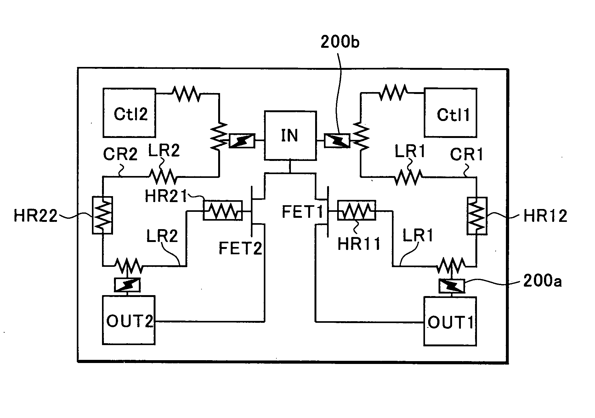
[0048] First, referring to FIGS. 1 to 5, the present invention will be described using an SPDT switch circuit device including two switching elements.
[0049]FIG. 1 is a circuit diagram illustrating a compound semiconductor switch circuit device. Source electrodes (or drain electrodes) of FETs (FET1 and FET2), which are two switching elements, are connected to a common input terminal IN. Gate electrodes of FET1 and FET2 are connected to a first control terminal Ctl1 and a second control terminal Ctl2 through a first connecting path and a second connecting path, respectively.
[0050] Further, the drain electrodes (or the source electrodes) of FET1 and FET2 are connected to a first output terminal OUT1 and a second output terminal OUT2, respectively. Control signals applied to the first and second control terminals Ctl1 and Ctl2 are complementary signals. Of the FETs, one to which an H-level signal is applied is turned on, whereby a high-frequency analog signal inputted to the common inp...
second embodiment
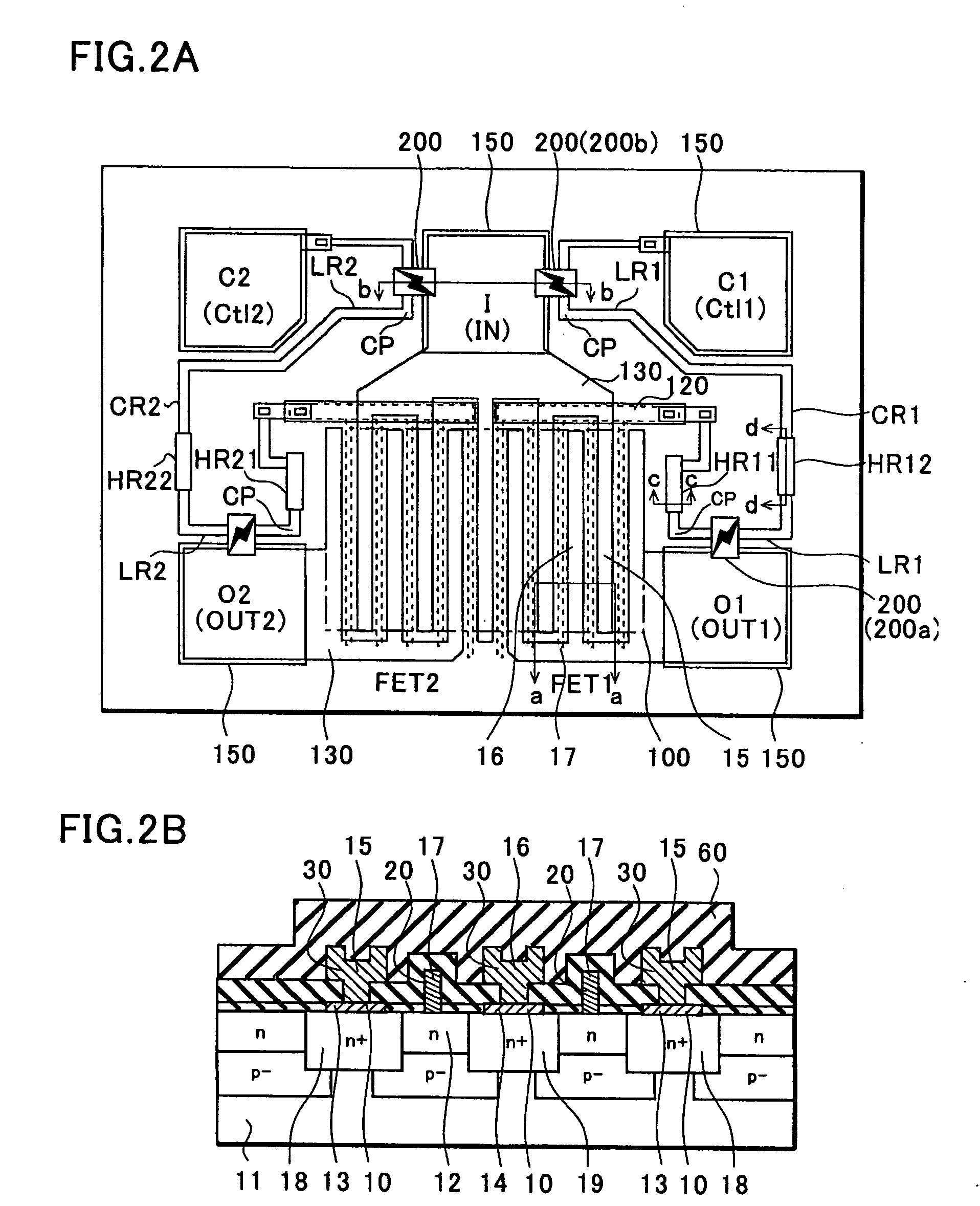
[0123] Referring to FIGS. 7A and 7B, the high-resistance elements of the second embodiment will be described. FIG. 7A is a cross-sectional view taken along line c-c of FIG. 2A, and FIG. 7B is a cross-sectional view taken along line d-d of FIG. 2A. Further, since the high-resistance elements HR11, HR12, HR21, and HR22 have similar structures, the high-resistance element HR11 will be described below.
[0124] The high-resistance element HR11 of this embodiment is a third conduction region isolated by the insulating region 50 and is constituted by a region in which the semiconductor layer under the cap layer 37 is exposed by removing the cap layer 37.
[0125] That is, the high-resistance element HR11 has a recess portion 101 in which the cap layer 37 is etched, and the cap layer 37 which serves as contact portions 102 for connection is left at both ends of the recess portion 101. The contact portions 102 are regions for continuously connecting directly to the cap layer 37 of the low-resist...
fourth embodiment
[0138]FIGS. 9A to 9C illustrate the present invention. FIG. 9A is a cross-sectional view taken along line d-d of FIG. 2A, FIG. 9B is a cross-sectional view taken along line b-b thereof, and FIG. 9C is a cross-sectional view taken along line a-a thereof.
[0139] In the fourth embodiment, an InGaP layer 40 is provided on a barrier layer 36 which is the same as the second embodiment, and a recess portions 101 are provided by etching a cap layer 37 and the InGaP layer 40. That is, the fourth embodiment has a structure in which the barrier layer 36 is exposed at bottom portions of the recess portions 101 of high-resistance elements HR11, HR12, HR21, and HR22.
[0140] In the third embodiment in which the InGaP layer 40 is similarly provided, since the InGaP layer 40 of high concentration also constitutes a resistive layer as well as a channel layer 35, there is the problem that the sheet resistance is slightly lower than that of the second embodiment. On the other hand, in the fourth embodim...
PUM
 Abstract
Description
Claims
Application Information