
Radio-frequency device

a radio frequency device and frequency technology, applied in the direction of antenna earthings, substantially flat resonant elements, resonance antennas, etc., can solve the problems of difficult to change the resonance frequency, difficulty in changing the parameters of those shapes and positions, and the degree of coupling with the power feed line, so as to achieve the desired radiation characteristics, the effect of optimizing the characteristics to be effective and easily setting or changing the characteristics of the devi

Active Publication Date: 2006-07-27
PANASONIC CORP
View PDF7 Cites 21 Cited by
  • Summary
  • Abstract
  • Description
  • Claims
  • Application Information

AI Technical Summary

Benefits of technology

[0016] Accordingly, an object of the present invention is to provide, for solving the above-described issues, a radio-frequency device which makes it implementable to easily set or change characteristics of the device after preparation of a basic device structure, and moreover which allows the optimization of the characteristics to be effectively achieved.
[0017] Another object of the present invention is to provide an antenna device design method which allows desired radiation characteristics to be simply obtained by using the radio-frequency device that is capable of changing the device characteristics.
[0051] According to the radio-frequency device of the present invention, after the basic structure of the device is prepared, characteristics such as the shape and position of the slot can be easily set and changed according to the conditions of use. In particular, by preparing the device basic structure as a common structure and by subjecting the structure to simple machining, device characteristics can be set or changed to desired ones so that efficient design and manufacture for such a radio-frequency device can be fulfilled. Furthermore, by setting the array period for individual conductive elements or the space width between neighboring conductive elements to specified conditions, the optimization of device characteristics can be effectively achieved, so that a radio-frequency device having successful radiation directivity can be provided.

Problems solved by technology

With such a design method, indeed the slot feeds power from the microstrip line having stable transmission characteristics over a broad band, but there is a problem that it is difficult to change the resonance frequency, degree of coupling with the power feed line and the like according to changes in conditions of use or the like after the preparation of the board, i.e., after the preparation of a basic structure of the antenna.
In such a structure, since the shapes and positional relation of the slot 707 and the patch 704 are invariable, there is a problem that it is difficult to change parameters of those shapes and positions after the preparation of the basic structure of the board.

Method used


Image

  • Radio-frequency device
  • Radio-frequency device
  • Radio-frequency device

Examples


embodiment

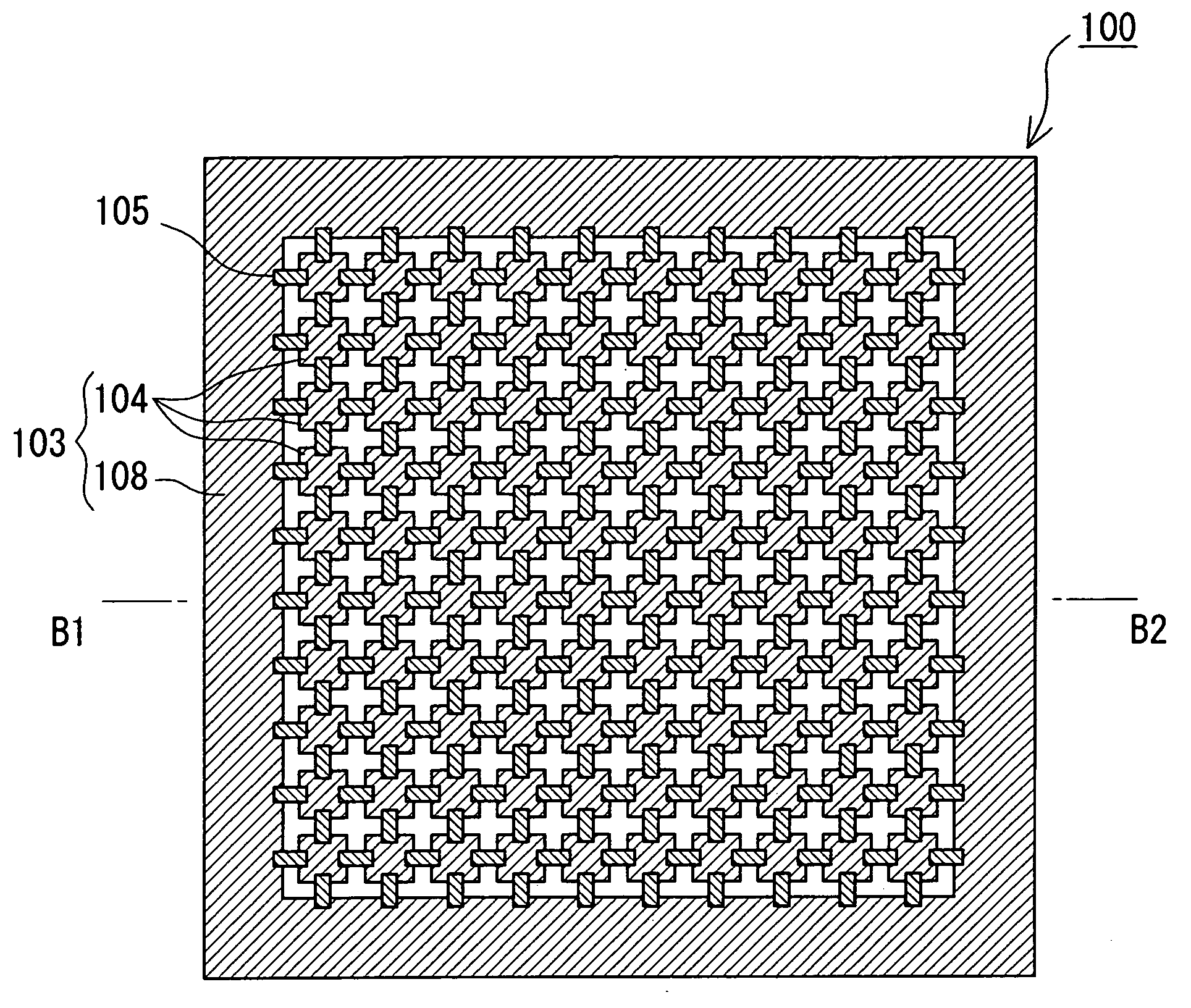
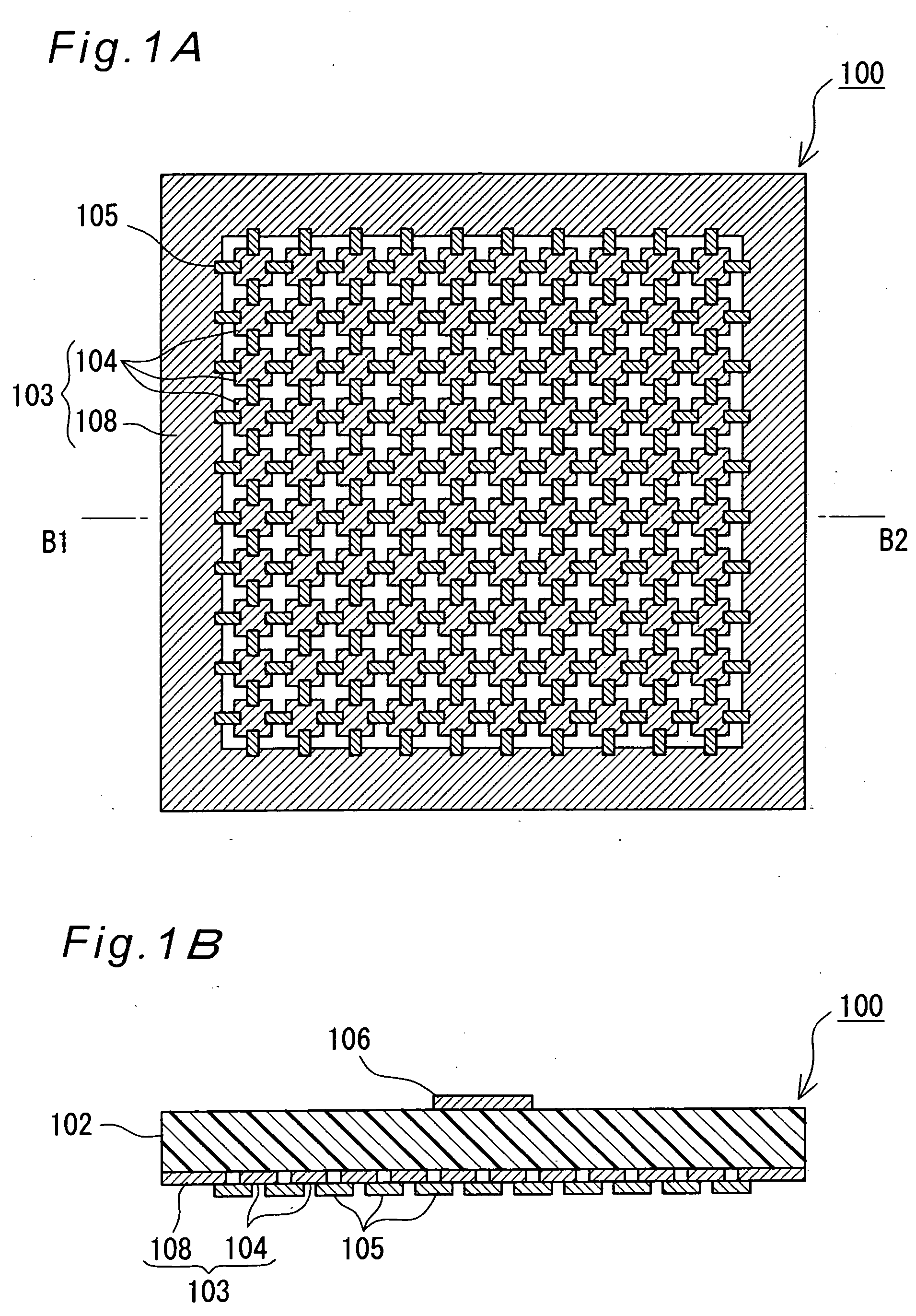
[0093]FIG. 1A is a schematic plan view showing a structure of a microstrip antenna device which is an example of the radio-frequency device according to an embodiment of the present invention, and FIG. 1B is a schematic sectional view taken along the line B1-B2 in the antenna device of FIG. 1A.

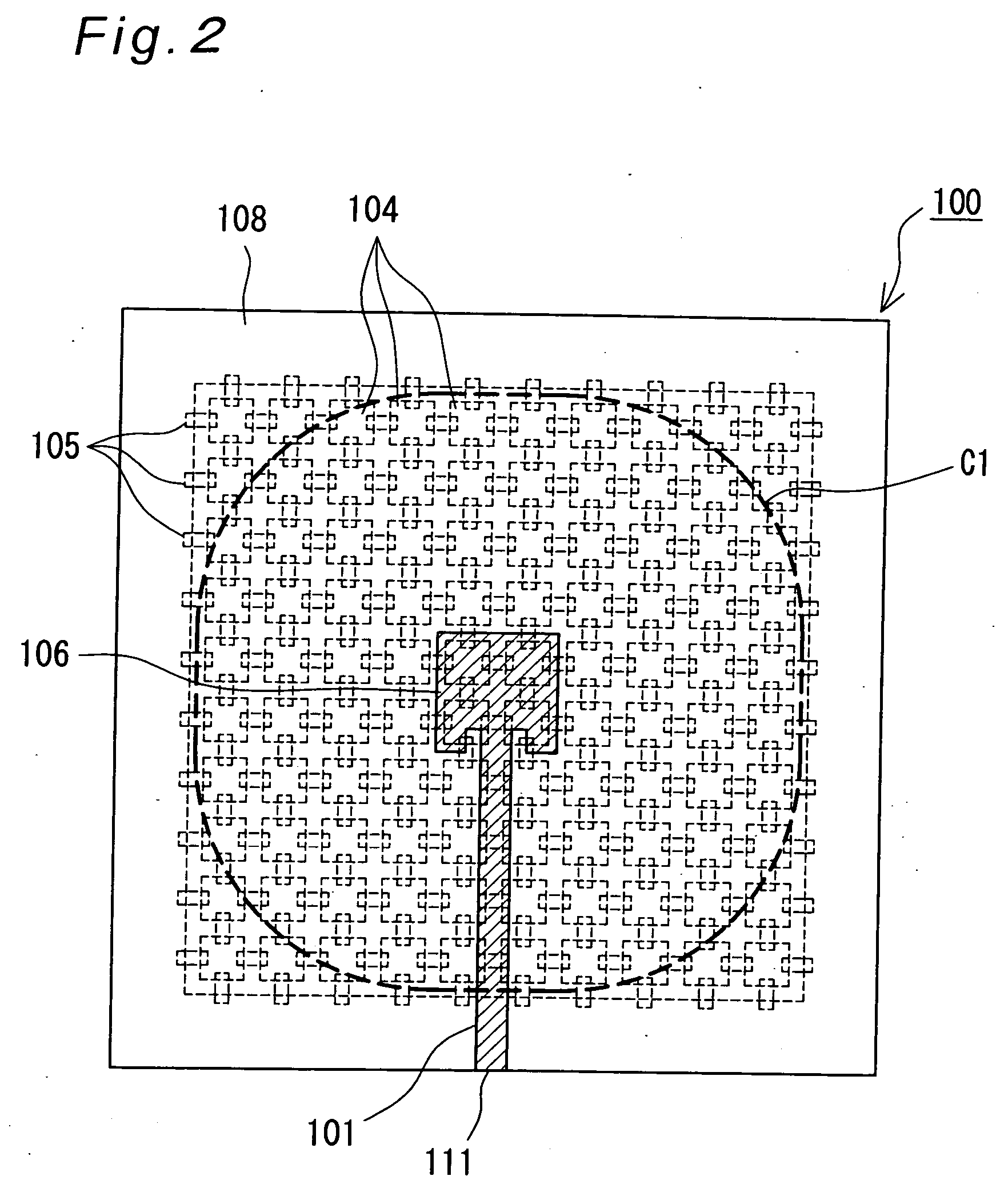
[0094] As shown in FIGS. 1A and 1B, a microstrip antenna device (or antenna board) 100 (hereinafter, abbreviated as an antenna device 100), which is an antenna device adopting a microstrip line structure, includes a generally square planar dielectric layer 102, a patch portion 106 which is an example of a first conductive layer formed on one surface of the dielectric layer 102, and a grounding conductive layer 103 which is an example of a second conductive layer formed on the other surface.

[0095] As shown in FIG. 1A, which is a schematic plan view as viewed from the grounding conductive layer 103 side in the antenna device 100, the grounding conductive layer 103 includes a conductive layer p...

example 1

[0134] Next, examples using such structures as described above will be described. As an antenna device according to this example, one using the slot prepared in the grounding conductive layer was used, and an electromagnetic field simulation and measurement of its return loss characteristics and radiation directivity were carried out.

[0135] The antenna device of this Example 1 was formed with its dielectric layer having a dielectric constant of 2.17 and a 140 mm×140 mm×1.6 mm dimensions, with the power feed line having a line width of 5.2 mm, and with the patch portion formed of a square shape (20 mm×20 mm) that resonates in TM01 mode at 5.0 GHz even under the condition that the grounding conductive layer was given by one continuous conductive layer. In this case, the effective wavelength A of the microstrip line is about 44 mm.

[0136] Also, in the grounding conductive layer, a conductive layer peripheral portion coupled with the external was provided in a peripheral portion, and a...


PUM


Abstract

In a radio-frequency device in which a dielectric layer, a first conductive layer and a second conductive layer are stacked one on another, the second conductive layer is including a plurality of conductive elements which are arrayed periodically and independently of one another at a specified array pitch, and a plurality of connecting elements for electrically connecting a plurality of mutually neighboring ones of the conductive elements to each other. The connection by the connecting elements is selectively made, thus making it possible to control radiation directivity of an electromagnetic field formed by the first and second conductive layers.

Description

[0001] This is a continuation application of International Application No. PCT / JP2005 / 012490, filed Jul. 6, 2005.BACKGROUND OF THE INVENTION [0002] 1. Field of the Invention [0003] The present invention relates to a radio-frequency device to be used in an apparatus using radio-frequency electromagnetic waves such as microwaves or millimeter waves. [0004] 2. Description of the Related Art [0005] It is known that a slot provided in a grounding conductor serves as an antenna equivalent to an electric dipole to radiate electromagnetic waves. By virtue of its low posture and simple structure, the slot can be utilized for electromagnetic coupling between multilayer boards, power feed to a radiator, or the like, thus lending itself to, for example, radio-frequency circuits in radio devices for use of communications. [0006] Meanwhile, there has been a prior art in which the slot is used in combination with an existing antenna technique to modify antenna characteristics as shown in, for exam...

Claims


Application Information

Patent Timeline
Patent Type & Authority Applications(United States)
IPC IPC(8): H01Q1/38
CPCH01Q1/38H01Q9/0407
Inventor FUJISHIMA, TOMOYASUSAKIYAMA, KAZUYUKISANGAWA, USHIOKANNO, HIROSHI
Owner PANASONIC CORP
Learn More