

Semiconductor light emitting device and manufacturing method thereof
- Summary
- Abstract
- Description
- Claims
- Application Information
AI Technical Summary
Benefits of technology
Problems solved by technology
Method used
Image

Examples
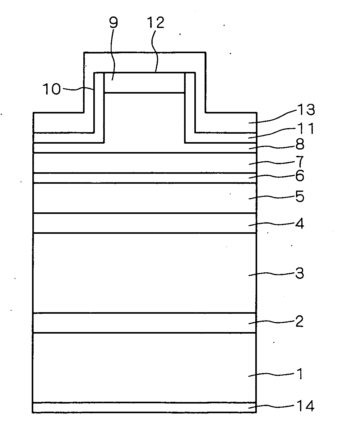
first embodiment
[0032] First, the characteristics of the semiconductor light emitting device according to this embodiment and the working effects thereof are described.
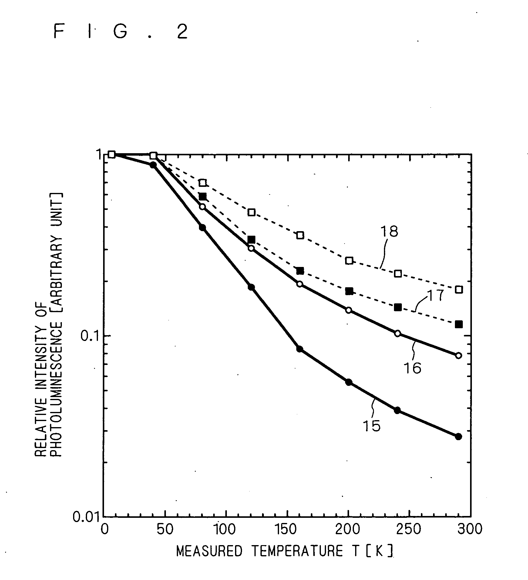
[0033] It is considered that the existence of spatial fluctuation in the In composition ratio in a quantum confined structure, such as a quantum well structure, makes the device properties, such as efficiency of light emission of a semiconductor light emitting device having a specific wavelength of emitted light, deteriorate in a GaN substrate where the density of penetration dislocations is low.
[0034] Thus, it is considered that the change in the light emission peak intensity (hereinafter in some cases simply referred to as “light emission intensity”) in the photoluminescence measurement corresponding to a change in the temperature directly reflects the degree of the spatial fluctuation in the In composition ratio in this quantum confined structure, as described below.
[0035] Therefore, it is considered that a quantum confined str...
PUM
 Abstract
Description
Claims
Application Information