Method and device for machining a wafer, in addition to a wafer comprising a separation layer and a support layer

a technology of separation layer and support layer, which is applied in the direction of solid-state device manufacturing, electric devices, semiconductor/solid-state device manufacturing, etc., can solve the problems of increasing the fragility and bend of thinned wafers, serious difficulties and challenges in subsequent treatment steps, and low thermal capacity, so as to reduce mechanical stresses, the adhesion and/or damping properties of the layer can be influenced and adjusted, and the effect of simplifying the coating of the rear sid

Active Publication Date: 2006-07-27
FRAUNHOFER GESELLSCHAFT ZUR FOERDERUNG DER ANGEWANDTEN FORSCHUNG EV
View PDF10 Cites 36 Cited by
  • Summary
  • Abstract
  • Description
  • Claims
  • Application Information

AI Technical Summary

Benefits of technology

[0033] The applied layer system (which comprises at least the interlayer and the carrier layer) should carry and / or protect the wafer surface during the subsequent processes, handling and transportation and, if necessary, should fix already divided components (wafer parts) until their desired removal and / or stripping. In this connection it is possible, in particular by adjusting the layer properties and material properties and / or the layer thickness, to adjust the layer so that it exhibits further advantages or matching properties. Thus, the flexibility, adhesion and / or the damping properties of the layer can be influenced and adjusted. In this connection it may be advantageous purposefully to embed and thereby protect the surface topography of the wafer. This may prove advantageous in particular with already bumped-up wafers, since in this way the projecting contacts are mechanically protected and in the subsequent thinning by means of grinding and / or abrasion the in general undesired penetrative forcing of the contacts is thus reduced or completely suppressed.
[0034] The applied layer system has several functions, some of which have already been disclosed in the preceding description. The layer system protects the front side of the wafer against mechanical and / or chemical or plasma technology damage during the thinning, reduces the mechanical stresses that are caused by the subsequent handling and transportation of the wafer, protects the front side of the wafer against impurities, serves as a sawing film, and is intended in particular to simplify the coating of the rear side. In this connection it is however unimportant whether the rear side coating process takes place before or after the division, or is omitted entirely.

Problems solved by technology

However, a small thickness provides not only advantages but also causes difficulties, especially in the further processing of the wafers: a greatly thinned wafer becomes increasingly fragile and bends due to stress in the function coating.
In addition it still has only a very low thermal capacity, which leads to serious difficulties and challenges for the subsequent treatment steps.
The greatly reduced mass and thus the likewise greatly reduced thermal capacity of the wafer means that the electrical circuits are significantly more highly loaded due to the high metallization temperatures.
In addition the handling of very greatly thinned wafers in conventional highly automated processes represents a challenge from the aspect of the mechanical stresses and further processability in existing handling equipment.
Up to now there has been no industrially implemented and satisfactory way of being able to provide a greatly thinned wafer with a rear side metallization, since all types of hitherto known carrier films break down on account of the necessary high metallization temperature.
All the coatings disclosed in the prior art are still not entirely satisfactory and for example in some cases can be separated again from the wafer only with a great deal of effort.
Furthermore the application of the layers is often complicated and the layer material is not optimally matched to the tasks it has to perform.
In this procedure the gas composition at the start of the plasma coating process is especially important: too high a residual oxygen content or too high a residual moisture (e.g. from wall deposits) leads to a marked, uncontrolled change of the gas composition and thus to a non-optimal first monolayer of the coating, which however must reproducibly produce the adhesion properties.
A non-optimal first monolayer of the coating may also occur if this layer is deposited during the transient phase of the plasma.
If a liquid precursor was used, this loses its property as a liquid release agent due to the aforedescribed crosslinking.
After the processing steps the wafer (and the chips produced therefrom) is generally extremely sensitive.

Method used


Image

  • Method and device for machining a wafer, in addition to a wafer comprising a separation layer and a support layer
  • Method and device for machining a wafer, in addition to a wafer comprising a separation layer and a support layer
  • Method and device for machining a wafer, in addition to a wafer comprising a separation layer and a support layer

Examples


example 2

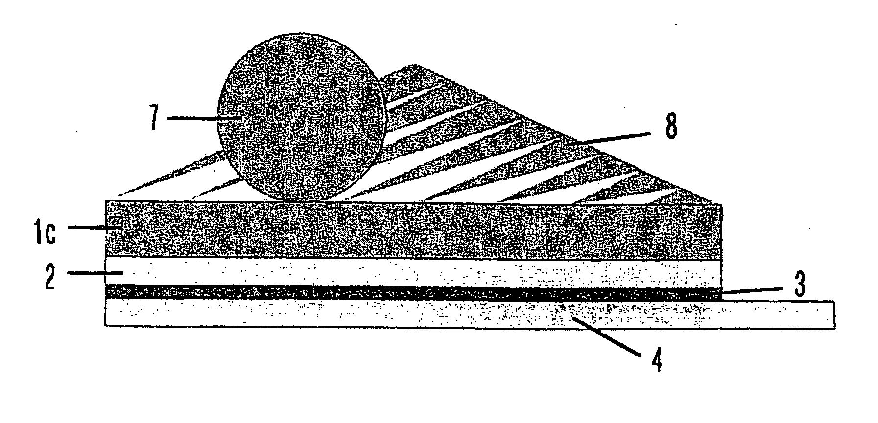
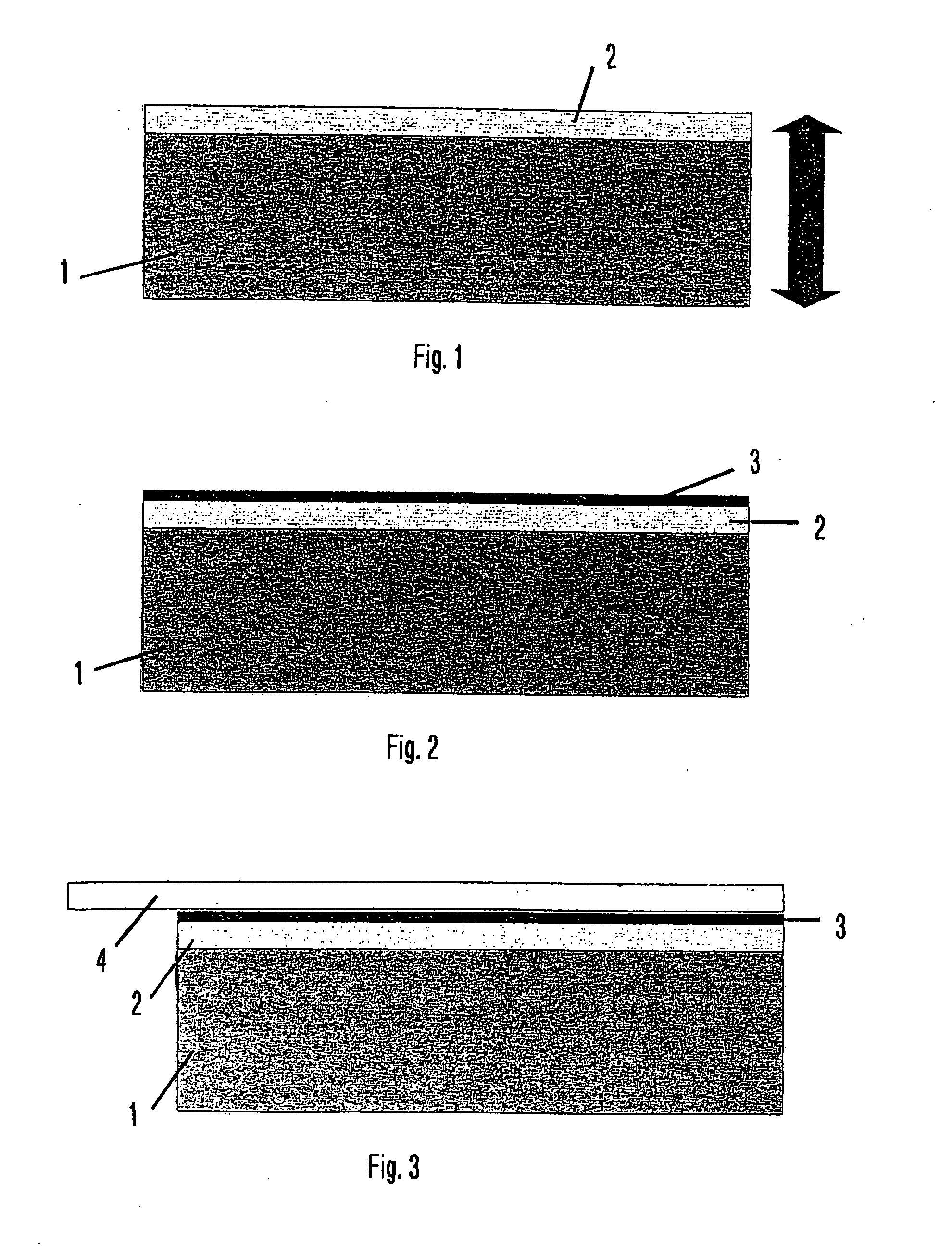
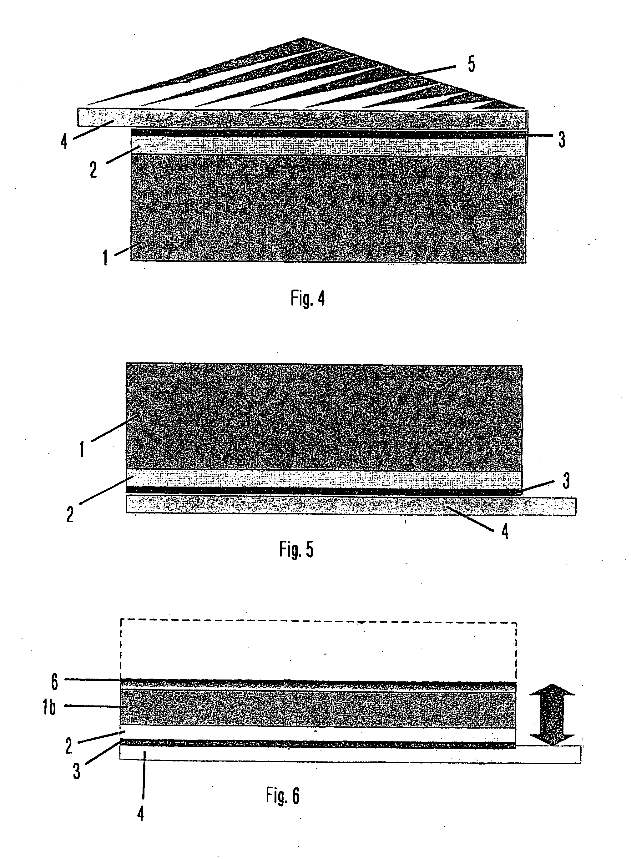
[0125] It is preferred if the wafer to be thinned and divided has, within a fabrication process for the production of ICs, transistors, diodes, sensors, etc., already passed through the majority of the fabrication steps for the application of the electrical and mechanical structures (components) and layers. The wafer is now covered or coated on the upper side (the active side, i.e. the side on which the structures are situated) with an interlayer and / or a carrier layer. The layer and / or the layer composite with the wafer arranged thereon is fixed on a carrier, for example by means of a film, and / or is held in situ by means of a vacuum suction device. Following this the wafer is fed into a unit system. The treatment process for thinning the wafer then takes place. In this way the thickness of the wafer is reduced by means of known methods such as for example grinding, lapping and / or etching.

[0126] The wafer can be cleaned during or following this process step. In addition a chemical...

example 3

Application of an Interlayer as Gradient Layer Using a Liquid Precursor

[0192] A linear polydimethylsiloxane of chain length 50 (AK 50, Wacker Chemie) was used as liquid precursor, which was applied in a layer thickness of 50 nm uniformly to a silicon wafer to be treated. In preliminary tests the material AK 50 exhibited a high resistance in vacuo. The prepared wafer was then introduced into a plasma polymerisation unit and coated further, employing the parameters listed in Table 1. In this connection the wafer was covered with an auxiliary device during part 1 of the coating procedure, which was removed at the start of part 2. The covering served to produce stable plasma and gas conditions before the wafer was exposed to the plasma. Typically, a transient phase in fact occurs at the start of a plasma process, which can have undesirable influences on the interface and / or on the liquid precursor (see also above).

TABLE 1Parameters during deposition of the interlayer;total layer thic...

example 4

Application of an Interlayer Thinner than the Gradient Layer Using a Liquid Precursor

[0195] Procedure as in Example 3; parameters, see Table 2.

TABLE 2Parameters during deposition of the interlayer;total layer thickness: ca 160 nmGas 1Gas 2Gas 3[sccm][sccm][sccm]Gas typeOutputTimePressureHMDSOO2H2[W][sec][mbar]Part 170247009000.03Part 2702470018000.03Part 320090016001800.05Part 41000025001200.22


PUM


Abstract

A process and an apparatus are described for the treatment of wafers, in particular for the thinning of wafers. A wafer with a carrier layer and an interlayer arranged between the carrier layer and the wafer is also described, in which the interlayer is a plasmapolymeric layer that adheres to the wafer and adheres more strongly to the carrier layer than to the wafer.

Description

FIELD OF APPLICATION [0001] A first aspect of the present invention relates to processes and apparatus for the treatment of wafers. These processes and apparatus are intended to facilitate the fabrication in a thinner format of the wafers used in the production of semiconductor products. In this connection the wafers should preferably be able to be treated more reliably and / or the necessary fabrication expenditure in the production of semiconductor components and / or circuits and / or sensors and / or other semiconductor products should be reduced and / or made more cost-effective and / or the use of laser cutting methods should be permitted or facilitated and / or, in particular, the coating and / or structuring of the rear side of the thinned wafer should be permitted or facilitated and / or the danger of fracturing and / or mechanical damage should be reduced. [0002] A further, closely related aspect of the invention relates to wafers with an interlayer and a carrier layer (covering layer). The f...

Claims


Application Information

Patent Timeline
Patent Type & Authority Applications(United States)
IPC IPC(8): H01L21/78H01L21/301H01L21/46
CPCH01L21/6836H01L2221/68327H01L2221/6834H01L2221/68395H01L21/78
Inventor JAKOB, ANDREASVISSING, KLAUS-D.STENZEL, VOLKMAR
Owner FRAUNHOFER GESELLSCHAFT ZUR FOERDERUNG DER ANGEWANDTEN FORSCHUNG EV
Why Eureka
Try Eureka