

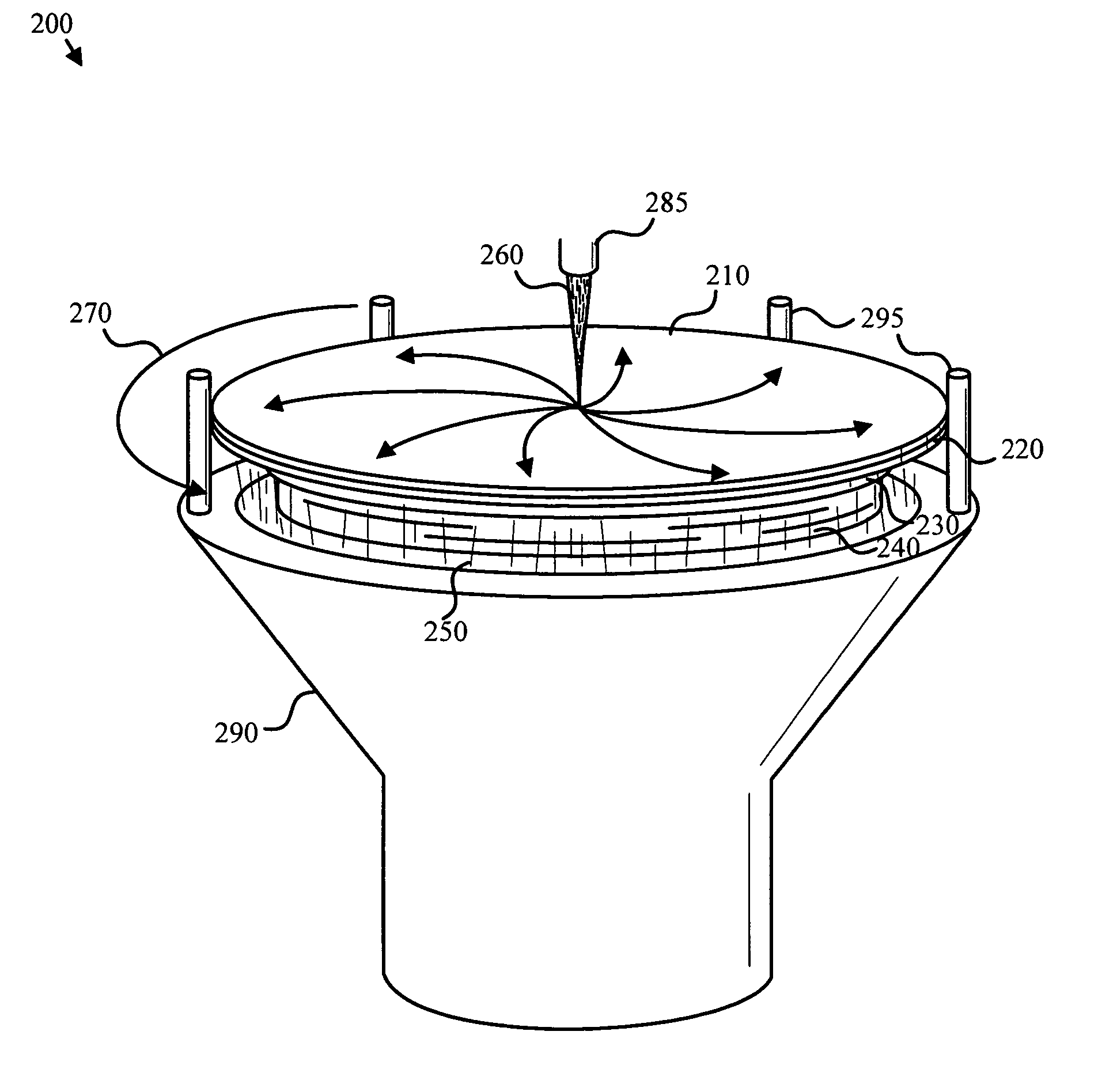
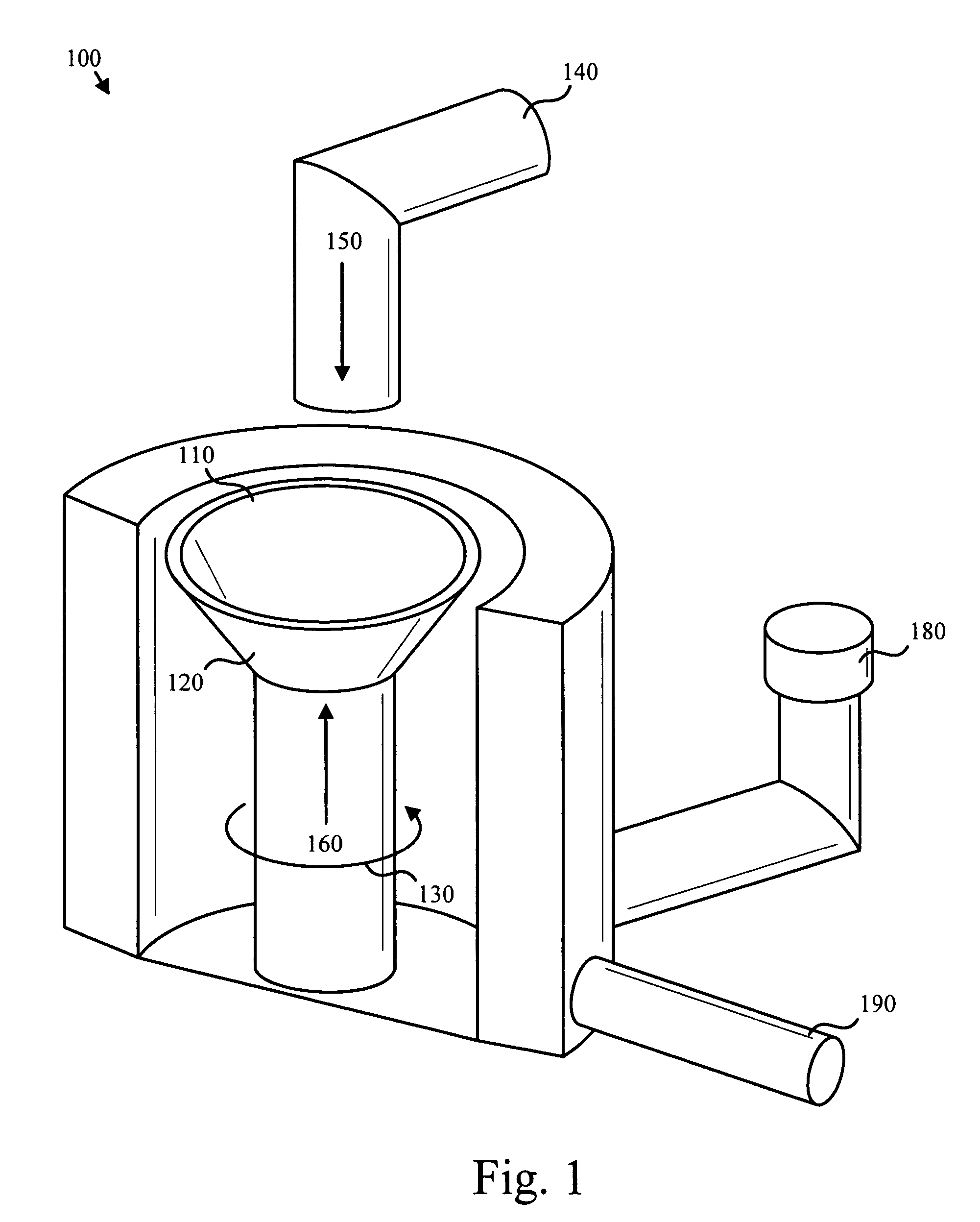
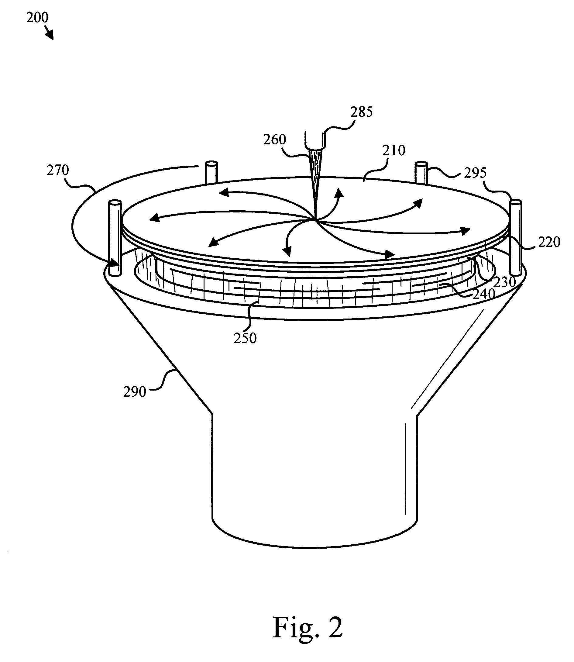
Apparatus, system, and method for reducing integrated circuit peeling
a technology of integrated circuit and peeling, applied in the field of apparatus, system and method for reducing integrated circuit peeling, can solve the problems of cross contamination, serious problems to the functionality of the integrated circuit and purity of the processing environment, and often collect unwanted film around the perimeter of the wafer, so as to effectively remove unwanted film, improve etching controllability and efficiency, and eliminate the effect of integrated circuit peeling
- Summary
- Abstract
- Description
- Claims
- Application Information
AI Technical Summary
Benefits of technology
Problems solved by technology
Method used
Image

Examples
Embodiment Construction
[0028] Reference throughout this specification to “one embodiment,”“an embodiment,” or similar language means that a particular feature, structure, or characteristic described in connection with the embodiment is included in at least one embodiment of the present invention. Thus, appearances of the phrases “in one embodiment,”“in an embodiment,” and similar language throughout this specification may, but do not necessarily, all refer to the same embodiment.
[0029] Furthermore, the described features, structures, or characteristics of the invention may be combined in any suitable manner in one or more embodiments. In the following description, numerous specific details are provided, to provide a thorough understanding of embodiments of the invention. One skilled in the relevant art will recognize, however, that the invention may be practiced without one or more of the specific details, or with other methods, components, materials, and so forth. In other instances, well-known structur...
PUM
| Property | Measurement | Unit |
|---|---|---|
| Height | aaaaa | aaaaa |
| Speed | aaaaa | aaaaa |
| Hydrophilicity | aaaaa | aaaaa |
Abstract
Description
Claims
Application Information