Substrate structure of liquid crystal display and method of forming alignment layer

a liquid crystal display and substrate structure technology, applied in the direction of instruments, nuclear engineering, transportation and packaging, etc., can solve the problems of poor uniformity of the alignment layer and the difficulty of controlling the profile of the alignment layer, so as to improve the displaying quality of the liquid crystal display, improve the uniformity of the layer, and improve the film properties

Inactive Publication Date: 2006-08-03
AU OPTRONICS CORP
View PDF26 Cites 25 Cited by
  • Summary
  • Abstract
  • Description
  • Claims
  • Application Information

AI Technical Summary

Benefits of technology

[0042] In the method of forming the alignment layer of the present invention, a hydrophilic layer is formed on the surface of the substrate of the display area and / or a hydrophobic layer is formed on the surface of the substrate of the non-display area. By using the hydrophilic and / or hydrophobic layer to define the area of the alignment layer, the uniformity of the layer can be achieved. As a result, the method of forming the alignment layer according to the present invention provides better film properties for the alignment layer, and thus the displaying quality of the liquid crystal display is improved.

Problems solved by technology

One issue of this method is the poor uniformity of the alignment layer.
In addition, it is hard to control the profile of the alignment layer.

Method used


Image

  • Substrate structure of liquid crystal display and method of forming alignment layer
  • Substrate structure of liquid crystal display and method of forming alignment layer
  • Substrate structure of liquid crystal display and method of forming alignment layer

Examples


first embodiment

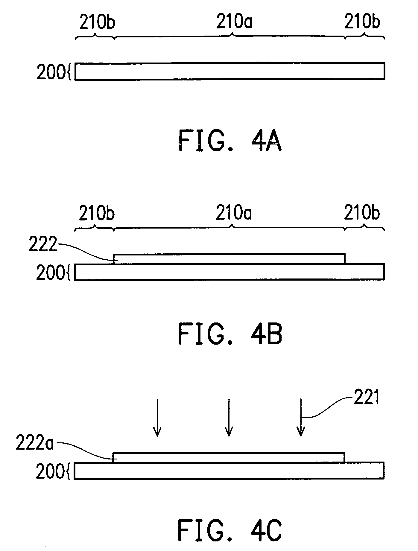
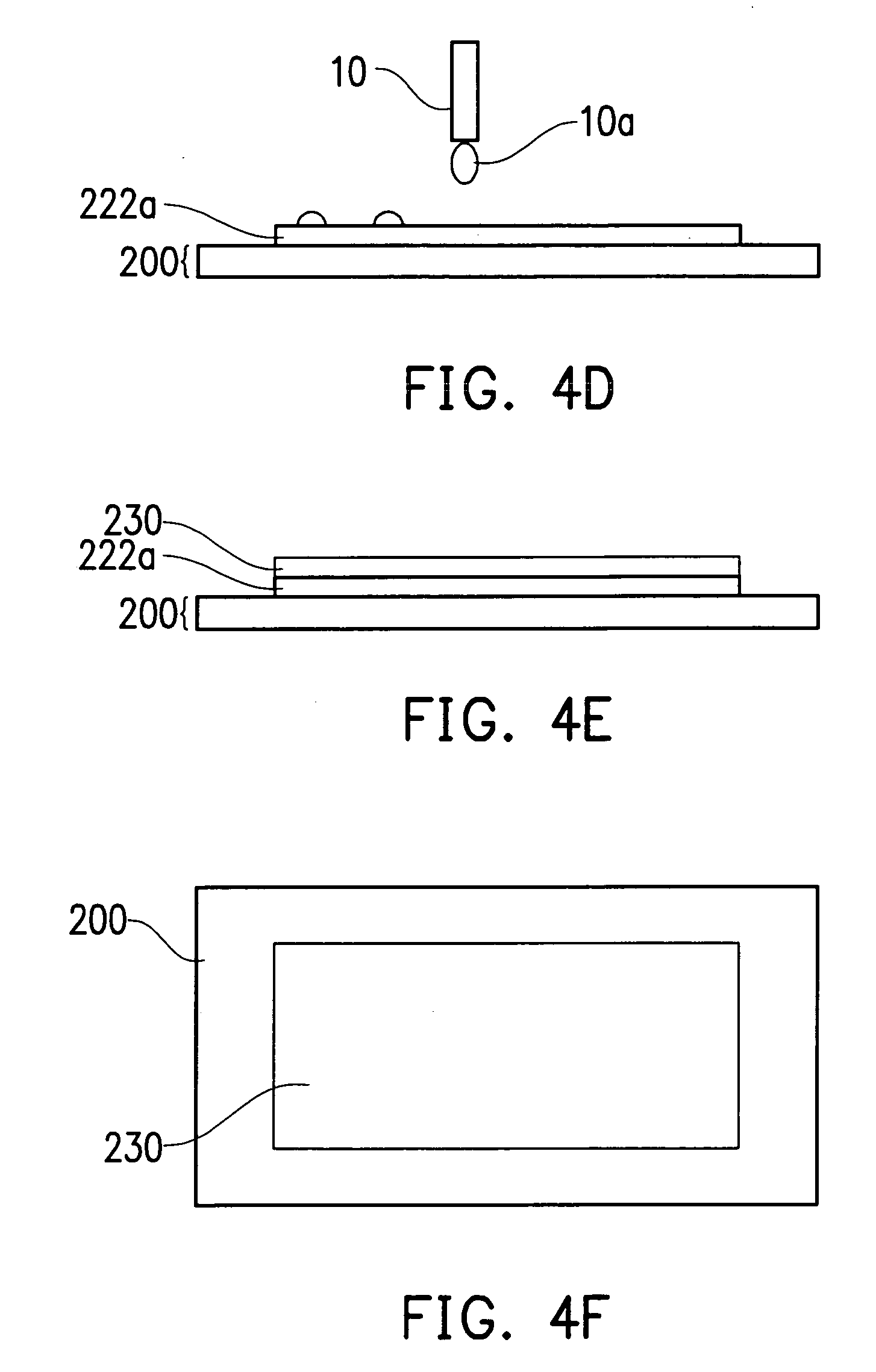
[0055]FIGS. 4A-4E are cross sectional views showing a method of forming an alignment layer according to a first embodiment of the present invention. Referring to FIG. 4A, a substrate 200 is first provided. The substrate 200 comprises a display area 210a and a non-display area 210b. In an embodiment, the substrate 200 can be, for example, a thin film transistor array substrate which comprises, for example, thin film transistors (TFTs), indium-tin-oxide (ITO) pixel electrodes, scan lines and data lines. In another embodiment, the substrate 200 can be, for example, a color filter substrate which comprises red, green and blue resins, black matrixes (BMs) and common electrodes.

[0056] Then, a hydrophilic layer 222a is formed on the surface of the substrate 200 of the display area 210a. In a preferred embodiment, the method of forming the hydrophilic layer 222a is described below. Referring to FIG. 4B, a silicon oxide layer 222 is first deposited on the substrate 200, for example, by a ch...

second embodiment

[0063]FIGS. 5A-5E are cross sectional views showing a method forming an alignment layer according to a second embodiment of the present invention. Referring to FIG. 5A, a substrate 200 is first provided. The substrate 200 comprises a display area 210a and a non-display area 210b. The substrate 200 can be, for example, a thin film transistor array substrate or a color filter substrate.

[0064] Then, a hydrophobic layer 242a is formed on the substrate 200 of the non-display area 210b. In a preferred embodiment, the method of forming the hydrophobic layer 242a is described below.

[0065] Referring to FIG. 5B, first a material layer 242 is deposited on the substrate 200, for example, by a plasma-enhanced chemical vapor deposition (PECVD) method. The material layer 242 can be, for example, a polysilicon layer, an amorphous silicon layer, a silicon nitride layer, or a combination thereof. A photolithographic process and an etching process are then performed to remain the material layer 242 ...

third embodiment

[0071] This embodiment is an application of combining the processes of the first embodiment and the second embodiment. FIGS. 6A-6F are cross sectional views showing a method of forming an alignment layer according to a third embodiment of the present invention. Referring to FIGS. 6A and 6B, which show the steps of forming the patterned silicon oxide layer 222, as described in the first embodiment. Referring to FIG. 6C, it shows forming the patterned material layer 242 in the non-display area 210b, as described in the second embodiment.

[0072] Referring to FIG. 6D, a treatment step 221 is performed to the silicon oxide layer 222 in the display area 210a and the material layer 242 in the non-display area 210b so that the silicon oxide layer 222 becomes a hydrophilic layer 222a and the material layer 242 becomes a hydrophobic layer 242a. The treatment step 221 can be, for example, a UV light exposure process, a laser process or a plasma process. The hydrophilic layer 222a and the hydro...


PUM

PropertyMeasurementUnit
areaaaaaaaaaaa
hydrophilicaaaaaaaaaa
hydrophobicaaaaaaaaaa

Abstract

A method of forming an alignment layer is described. A substrate comprising a display area and a non-display area is provided. A hydrophilic layer is formed on the substrate of the display area. A solution of an alignment material is dropped on the hydrophilic layer. The solution of the alignment material is solidified to form an alignment layer. Before dropping the solution of the alignment material on the hydrophilic layer, a hydrophobic layer may be formed on the substrate of the non-display area.

Description

CROSS-REFERENCE TO RELATED APPLICATION [0001] This application claims the priority benefit of Taiwan application serial no. 94103171, filed on Feb. 2, 2005. All disclosure of the Taiwan application is incorporated herein by reference. BACKGROUND OF THE INVENTION [0002] 1. Field of the Invention [0003] The present invention relates to a substrate structure of a liquid crystal display and a method of forming an alignment layer, and more particularly, to a method of forming an alignment layer in which a uniform alignment layer can be obtained. [0004] 2. Description of the Related Art [0005] Recently, liquid crystal display devices which are slim and low-power consuming have been widely applied to personal computers, mobile phones, personal digital assistants, televisions, video cameras, and measuring instruments. Generally, a liquid crystal display is composed of two substrates and a liquid crystal layer between them. Regardless of an active matrix liquid crystal or a passive matrix li...

Claims


Application Information

Patent Timeline
Patent Type & Authority Applications(United States)
IPC IPC(8): C09K19/00B05D5/12
CPCY10T428/1045G02F1/133711C09K2323/033
Inventor TUNG, YUAN-HUNGPAN, CHIH-JUI
Owner AU OPTRONICS CORP
Why Eureka
Try Eureka