Sealing pores of low-k dielectrics using CxHy

a dielectric and low-k technology, applied in the field of forming and processing of porous, low-k dielectrics, can solve the problems of plasma damage, low-k materials are susceptible to damage, and low-k materials present problems during processing

Inactive Publication Date: 2006-08-03
TAIWAN SEMICON MFG CO LTD
View PDF22 Cites 405 Cited by
  • Summary
  • Abstract
  • Description
  • Claims
  • Application Information

AI Technical Summary

Benefits of technology

[0012] These and other problems are generally solved or circumvented and technical advantages are generally achieved by preferred embodiments of the present invention that provides a method for repairing low-k dielectrics suffering from pore damage or carbon depletion.

Problems solved by technology

However, low-k materials present problems during processing, especially during the processing of the conductive material used to make interconnects.
The low-k materials are susceptible to damage from a plasma etch because they are softer, less chemically stable or more porous, or any combination of these factors.
The plasma damage can manifest itself in higher leakage currents, lower breakdown voltages, and changes in the dielectric constant associated with the low-k dielectric material.
In addition, the damaged OSG material has been observed to adsorb moisture.
It has also been observed that this degraded low-k dielectric material is vulnerable to chemical attack during exposure to wet chemical cleanups, which results in significant critical dimension (CD) loss of low-k dielectric film insulating structures.
Just as with carbon containing dielectrics, porous dielectrics are also susceptible to damage from plasma etching and ashing processes used in device fabrication.
When there is an open pore in the dielectric, processing fluids in lap and polish and in thin film metallization can enter surface pores, thereby causing corrosion, mechanical damage, or an increase in the dielectric constant.
As noted above, dielectric damage causes higher leakage currents, lower breakdown voltages, and changes in the dielectric constant associated with the low-k dielectric material.

Method used


Image

  • Sealing pores of low-k dielectrics using CxHy
  • Sealing pores of low-k dielectrics using CxHy
  • Sealing pores of low-k dielectrics using CxHy

Examples


Embodiment Construction

[0028] The operation and fabrication of the presently preferred embodiments are discussed in detail below. However, the embodiments and examples described herein are not the only applications or uses contemplated for the invention. The specific embodiments discussed are merely illustrative of specific ways to make and use the invention, and do not limit the scope of the invention or the appended claims.

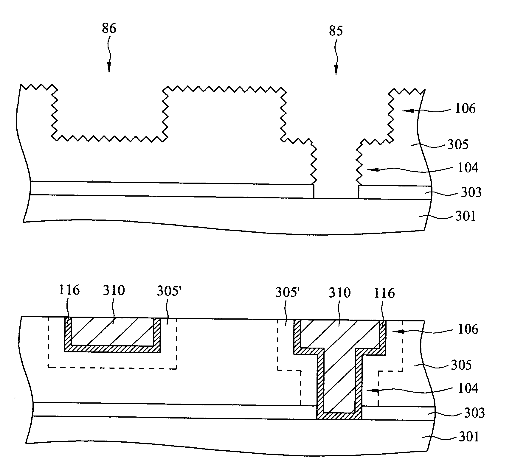
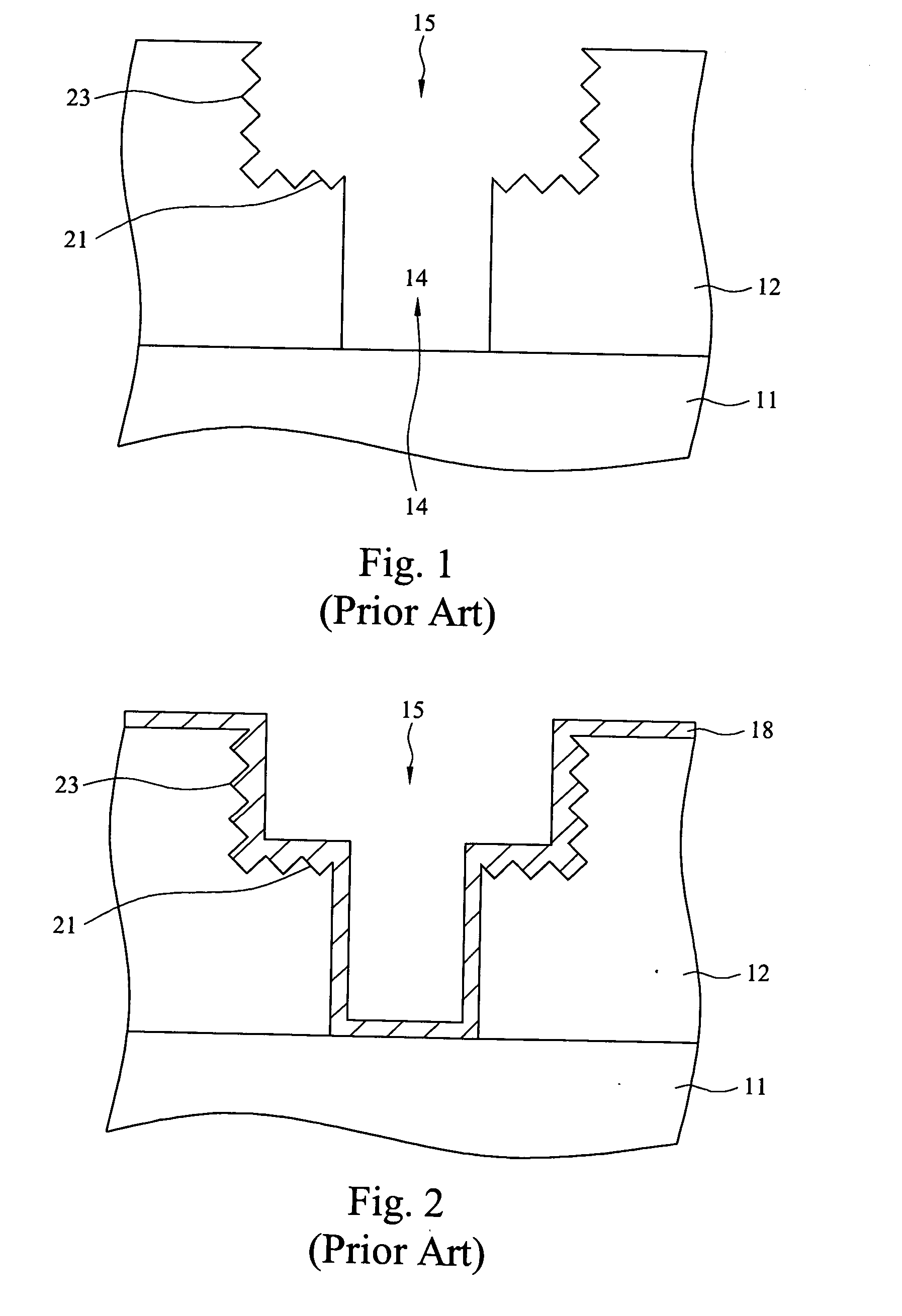
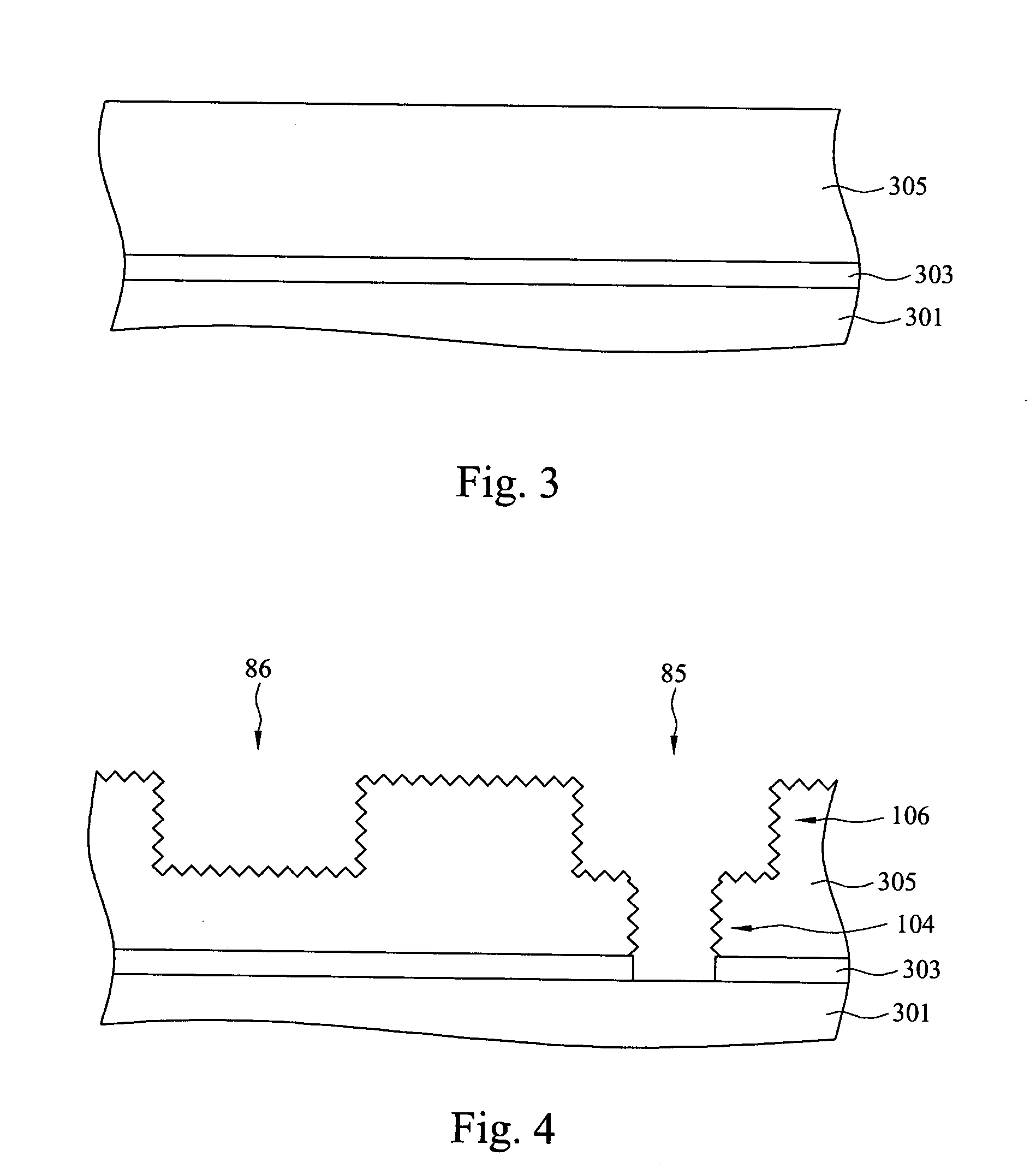
[0029] This invention relates generally to semiconductor device manufacturing and more particularly to the formation and processing of porous, low-k dielectrics. The low-k dielectrics may include films or layers, but embodiments are not limited to these morphologies. The present invention will now be described with respect to preferred embodiments in a specific context, namely the creation of copper conductive lines and vias in the damascene process. It is believed that embodiments of this invention are particularly advantageous when used in this process. It is further believed that ...


PUM

PropertyMeasurementUnit
dielectric constantsaaaaaaaaaa
thicknessaaaaaaaaaa
dielectric constantaaaaaaaaaa

Abstract

A semiconductor method of manufacturing involving porous and/or carbon containing, low-k dielectrics is provided. The method includes forming a hydrocarbon of the general composition CxHy on the surface of the low-k dielectric. The hydrocarbon layer includes depositing a precursor material, preferably C2H4 or (CH3)2CHC6H6CH3. In accordance with embodiments of this invention, carbon diffuses into the low-k dielectric, thereby reducing carbon depletion damage caused by plasma processing or etching. Surface dielectric pores damaged by plasma processing are also repaired by sealing them with the CXHY layer. Embodiments include semiconductor devices, such as devices having damascene interconnect structures, manufacturing using methods provided.

Description

CROSS-REFERENCE TO RELATED APPLICATIONS [0001] This application relates to co-pending and commonly assigned patent application Ser. No. xx / xxx,xxx (TSM04-0867), filed concurrently herewith, entitled “CxHy Sacrificial Layer for Cu / Low-K Interconnects.” This application also relates to co-pending and commonly assigned patent application Ser. No. 10 / 985,149 (TSM04-0369), filed Nov. 10, 2004, entitled “Diffusion Barrier for Damascene Structures.” These co-pending and commonly assigned patent applications are hereby incorporated by reference. TECHNICAL FIELD [0002] This invention relates generally to semiconductor device manufacturing and more particularly to the formation and processing of porous, low-k dielectrics. BACKGROUND [0003] As the density of semiconductor devices increases and the size of circuit elements becomes smaller, the resistance capacitance (RC) delay time increasingly dominates the circuit performance. To reduce the RC delay, there is a desire to switch from conventio...

Claims


Application Information

Patent Timeline
Patent Type & Authority Applications(United States)
IPC IPC(8): H01L21/4763
CPCH01L21/76831
Inventor LIN, KENG-CHUCHENG, SHWANG-MINGYEH, MING LINGBAO, TIEN-I
Owner TAIWAN SEMICON MFG CO LTD
Why Eureka
Try Eureka