Semiconductor light-emitting device

a technology of semiconductors and light-emitting devices, which is applied in the direction of semiconductor devices, lasers, semiconductor lasers, etc., can solve the problems of poor conversion efficiency, inherently inefficient down-conversion process, and high energy-inefficiency of typical incandescent light sources

Inactive Publication Date: 2006-08-10
RGT UNIV OF CALIFORNIA
View PDF29 Cites 265 Cited by
  • Summary
  • Abstract
  • Description
  • Claims
  • Application Information

AI Technical Summary

Problems solved by technology

Typical incandescent light sources, while highly energy-inefficient, have a desirable characteristic broad-emission spectrum and a high color-rendering index.
The process of down-conversion is inherently inefficient due to the Stokes shift (a difference in transition energy of the emission and absorption spectra resulting from defects in the material and, in general, partial non-radiative decay) and poor conversion efficiency.
However, using indium-containing alloys to obtain long wavelength emission (blue to infrared) has its own problems; primary among them is that depositing layers with a high indium content causes significant degradation of the material quality, which is detrimental to device functioning and performance.
Thus, it is currently not possible to make very efficient nitride-based green, yellow or red light emitting diodes (LEDs), as well as lasers.
Further, current designs proposing methods to obtain “white” light without the aid of phosphors typically rely on a high-indium content layer deposited under conditions that result in poor material quality.

Method used


Image

  • Semiconductor light-emitting device
  • Semiconductor light-emitting device
  • Semiconductor light-emitting device

Examples


Embodiment Construction

[0027] In the following description of the preferred embodiment, reference is made to the accompanying drawings which form a part hereof, and in which is shown by way of illustration a specific embodiment in which the invention may be practiced. It is to be understood that other embodiments may be utilized and structural changes may be made without departing from the scope of the present invention.

[0028] Overview

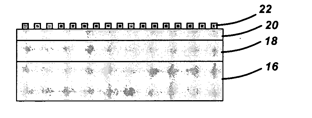
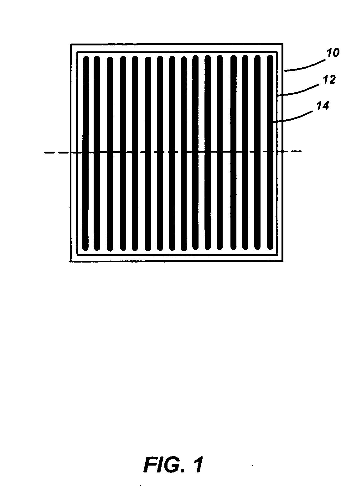
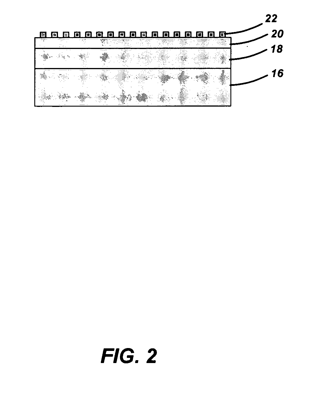
[0029] GaN-based light emitting diodes hold the promise of revolutionizing the lighting industry, thanks to their high efficiency and versatility. Similarly, GaN-based laser diodes have already had a significant impact on high-density data storage. Current state-of-the-art GaN-based semiconductor light emitting devices typically comprise an “active” region with a single-quantum-well or multiple-quantum-well structure emitting blue or near-UV light. This light may be used to excite a phosphor or combination of phosphors to produce secondary emission in the green / red / yellow ...


PUM


Abstract

A semiconductor light-emitting diode, and method of fabricating same, wherein an indium (In)-containing light-emitting layer, as well as subsequent device layers, is deposited on a textured surface. The resulting device is a phosphor-free white light source.

Description

CROSS-REFERENCE TO RELATED APPLICATIONS [0001] This application is related to the following co-pending and commonly-assigned applications: [0002] U.S. Utility application Ser. No. 10 / 938,704, filed Sep. 10, 2004, by Carole Schwach, Claude C. A. Weisbuch, Steven P. DenBaars, Henri Benisty, and Shuji Nakamura, entitled “WHITE, SINGLE OR MULTI-COLOR LIGHT EMITTING DIODES BY RECYCLING GUIDED MODES,” attorneys' docket number 30794.115-US-01 (2004-064-1), and [0003] P.C.T. International Application Serial No. US03 / 39211, filed Dec. 9, 2003, by Tetsuo Fujii, Yan Gao, Evelyn L. Hu, and Shuji Nakamura, entitled “HIGHLY EFFICIENT GALLIUM NITRIDE BASED LIGHT EMITTING DIODES VIA SURFACE ROUGHENING,” attorneys' docket number 30794.108-WO-U1 (2004-063-1), [0004] which applications are incorporated by reference herein.STATEMENT REGARDING SPONSORED RESEARCH AND DEVELOPMENT [0005] The present invention was made under support from the University of California, Santa Barbara Solid State Lighting and D...

Claims


Application Information

Patent Timeline
Patent Type & Authority Applications(United States)
IPC IPC(8): H01L33/00H01L33/22
CPCB82Y20/00H01L33/007H01L33/22H01S5/0207H01S5/10H01S5/1053H01S5/34333
Inventor SHARMA, RAJATPATTISON, PAUL MORGANKAEDING, JOHN FRANCISNAKAMURA, SHUJI
Owner RGT UNIV OF CALIFORNIA
Why Eureka
Try Eureka