Method for manufacturing SOI substrate

a technology of soi and substrate, which is applied in the direction of semiconductor/solid-state device manufacturing, basic electric elements, electric apparatus, etc., can solve the problems of increasing the incidence of crystal defects, and achieve the effects of reducing damage, enhancing the bonding strength of the bonded substrate, and uniform thickness of the soi layer

Active Publication Date: 2006-08-10
SUMCO CORP
View PDF3 Cites 26 Cited by
  • Summary
  • Abstract
  • Description
  • Claims
  • Application Information

AI Technical Summary

Benefits of technology

[0009] The object of the present invention is to provide a method for manufacturing an SOI substrate whereby it is possible to manufacture an SOI substrate in which the crystal integrity of the SOI layer is not seriously damaged, and the variation in thickness of the SOI layer is effectively suppressed, i.e., the thickness of the SOI layer becomes uniform.
[0010] As shown in FIG. 1, a first aspect of the present invention as described in claim 1 relates to a method for manufacturing an SOI substrate comprising the steps of forming an oxide film 21 at least on one surface of a first silicon substrate 14, implanting hydrogen ions from the surface of the first silicon substrate 14 thereby forming an ion-implantation zone 16 in the interior of the first silicon substrate 14, bonding the first silicon substrate 14 over a second silicon substrate 12 with the oxide film 21 interposed thereby forming a laminated assembly 15, subjecting the laminated assembly 15 to a first heating treatment consisting of heating at a specified temperature, so that the first silicon substrate 14 is split at the ion-implantation zone 16 thereby manufacturing a bonded substrate 18 in which a thin SOI layer 13 is formed on the second silicon substrate 12 with the oxide film 21 interposed, flattening the exposed surface of the SOI layer 13 by subjecting the bonded substrate 18 to wet etching, subjecting the bonded substrate 18 to a second heating treatment consisting of heating at 750 to 900° C. in an oxidative atmosphere thereby reducing damages inflicted to the SOI layer 13, and subjecting the resulting bonded substrate 18 to a third heating treatment consisting of heating at 900 to 1200° C. thereby enhancing the bonding strength of the bonded substrate 18.
[0011] According to the method described in claim 1 for manufacturing an SOI substrate, since the exposed surface of the SOI layer 13 is flattened by wet etching, it is possible not only to remove damages present on the surface of the SOI layer 13 coincident with the exposed surface of the ion-implantation zone 16 where the damages occur as a result of the first heating treatment, but also to avoid inflicting additional damages onto the exposed surface of the SOI layer 13, thereby reducing the variation in thickness of the SOI layer 13, and enhancing the uniformity of thickness of the SOI layer 13.

Problems solved by technology

In particular, if the bonded substrate is subjected directly to a heating treatment consisting of heating to 900° C. or higher, the oxidation reaction proceeds at such a high speed that a large number of interstitial silicon atoms will develop in a short period of time which will then increase the incidence of crystal defects.

Method used


Image

  • Method for manufacturing SOI substrate
  • Method for manufacturing SOI substrate

Examples


example 1

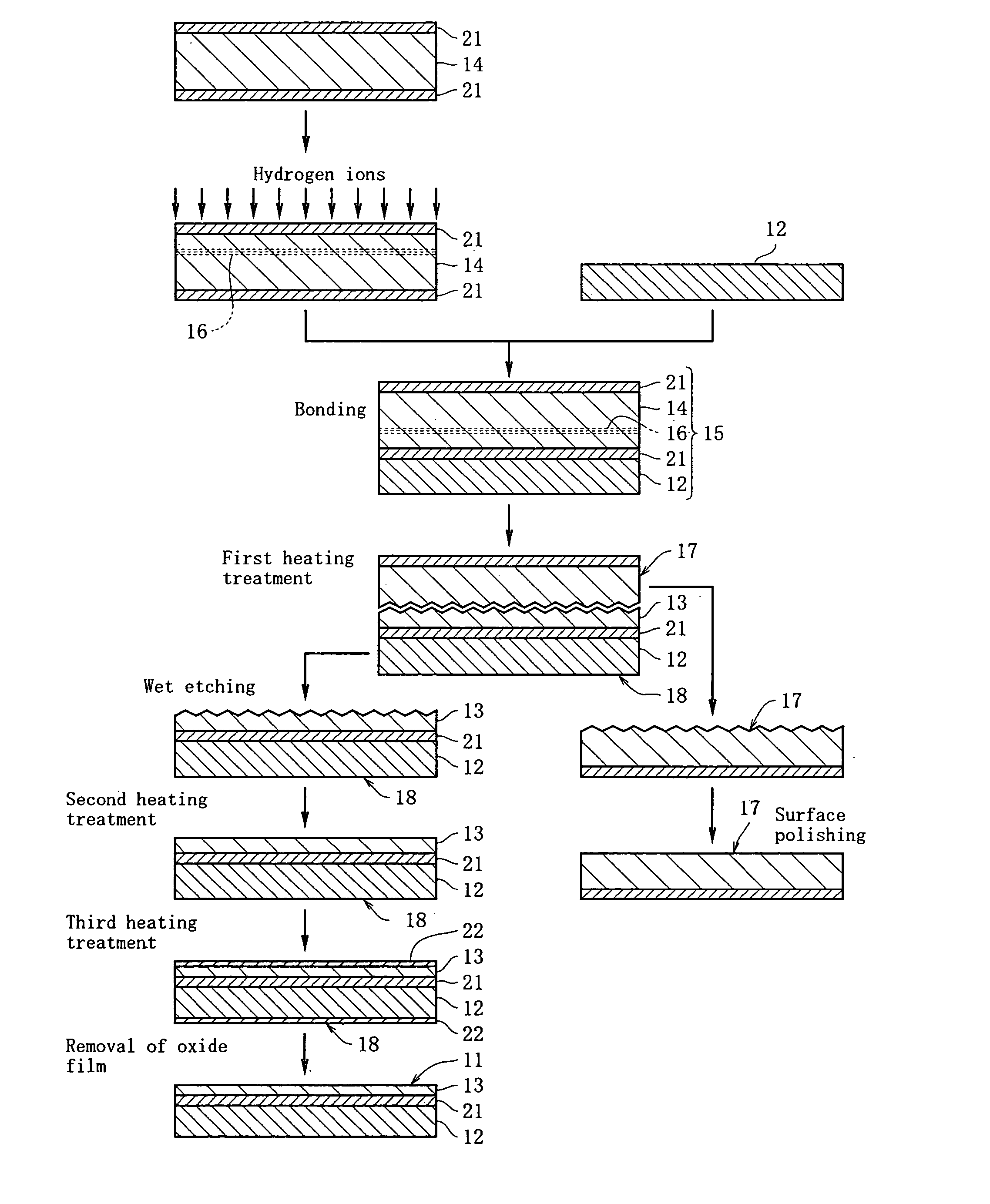
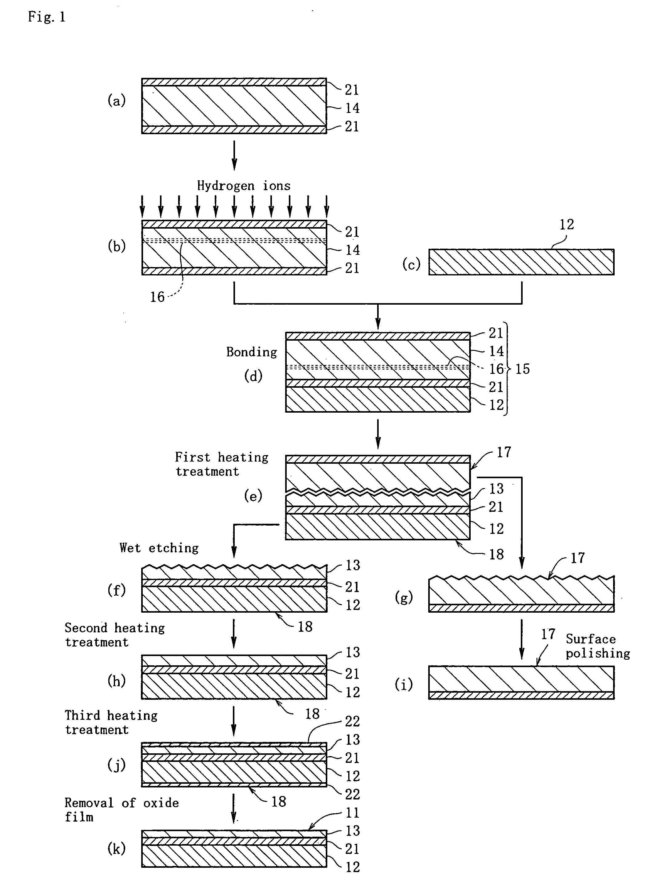
[0038] As shown in FIG. 1, first a disc-shaped (outer diameter, 200 mm and thickness, 0.725 mm) first silicon substrate 14 composed of silicon single crystal was subjected to a heating treatment consisting of heating at 1000° C. for 5 hours in an oxygen atmosphere, to allow a first oxide film 21 to be formed on the top and bottom surfaces of the first silicon substrate 14 as well as its side surfaces. The first oxide film 21 has a thickness of about 150 nm. Then, implantation of hydrogen ions into a surface of the first silicon substrate 14 was performed by radiating a beam of hydrogen ions at a dose of 6×10¹⁶ atoms / cm2 under an acceleration voltage of 50 keV. Through this operation, an ion-implantation zone 16 is formed in the interior of the first silicon substrate 14 (FIG. 1(b)). The depth of the ion-implantation zone 16 (in terms of the level at which the density of implanted hydrogen ions had a peak) from the top surface was determined to be about 500 nm with the thickness of f...

example 2

[0040] A bonded substrate 18 was subjected to wet etching so that SOI layer 13 was thinned until its thickness was 300 nm. Not being subjected to a second heating treatment consisting of heating at 900° C., the bonded substrate 18 was immediately subjected to a heating treatment consisting of heating at 1100° C. for 120 minutes in an atmosphere of argon. Except for this alteration, the bonded substrate 18 was processed in the same manner as in Example 1 to manufacture an SOI substrate. This SOI substrate was made Example 2.

example 3

[0041] Not being subjected to wet etching, a bonded substrate 18 immediately received a second heating treatment consisting of heating at 900° C. for 90 minutes in an oxygen atmosphere, and third heating treatment consisting of heating at 1100° C. for 120 minutes in an oxygen atmosphere in this order. Except for this alteration, the bonded substrate 18 was processed in the same manner as in Example 1 to manufacture an SOI substrate. This SOI substrate was made Example 3.


PUM

PropertyMeasurementUnit
thicknessaaaaaaaaaa
temperatureaaaaaaaaaa
thicknessaaaaaaaaaa

Abstract

The object of the invention is to provide a method for manufacturing an SOI layer which is devoid of damages, has a reduced variation in thickness, and is uniform in thickness. The object is met by providing a method for manufacturing an SOI substrate comprising the steps of forming an oxide film at least on one surface of a first silicon substrate, implanting hydrogen ions from the surface of the first silicon substrate thereby forming an ion-implantation zone in the interior of the first silicon substrate, bonding the first silicon substrate over a second silicon substrate with the oxide film interposed thereby forming a laminated assembly, subjecting the laminated assembly to a first heating treatment consisting of heating at a specified temperature, so that the first silicon substrate is split at the ion-implantation zone thereby manufacturing a bonded substrate, flattening the exposed surface of the SOI layer by subjecting the bonded substrate to wet etching, subjecting the bonded substrate to a second heating treatment consisting of heating at 750 to 900° C. in an oxidative atmosphere thereby reducing damages inflicted to the SOI layer, and subjecting the resulting bonded substrate to a third heating treatment consisting of heating at 900 to 1200° C. thereby enhancing the bonding strength of the bonded substrate.

Description

CROSS-REFERENCES TO RELATED APPLICATIONS [0001] This application claims priority of Japanese Application No. 2005-025802 filed Feb. 4, 2005, the entire disclosure of which is hereby incorporated by reference. BACKGROUND OF THE INVENTION [0002] 1. Field of the Invention [0003] The present invention relates to a method for manufacturing an SOI (silicon on insulator) substrate wherein an SOI layer is formed on an oxide film using hydrogen ion-implantation technique. [0004] 2. Description of the Related Art [0005] A method has been proposed for manufacturing an SOI substrate (for example, see Patent Document 1). The method comprises forming an oxide film on a surface of a first silicon substrate, implanting a high concentration of hydrogen atoms into the interior of the silicon substrate to form an ion-implantation zone at a specified depth from the surface of the substrate, bonding the first silicon substrate over a second silicon substrate to form a laminated assembly, heating the lam...

Claims


Application Information

Patent Timeline
Patent Type & Authority Applications(United States)
IPC IPC(8): H01L21/30H01L21/46
CPCH01L21/76254
Inventor ENDO, AKIHIKOKUSABA, TATSUMIOKUDA, HIDEHIKOMORITA, ETSUROU
Owner SUMCO CORP
Why Eureka
Try Eureka