Flash memory cell with UV protective layer

a technology of flash memory and protective layer, which is applied in the direction of semiconductor devices, semiconductor/solid-state device details, electrical apparatus, etc., can solve the problems of charge buildup in the charge storage layer, subsequent increases in v/sub>t/sub>, and charge buildup and concomitant increase in v, so as to reduce the thickness variation in the topography of the ild, the effect of easy adaptation

Active Publication Date: 2006-01-24
INFINEON TECH LLC
View PDF9 Cites 9 Cited by
  • Summary
  • Abstract
  • Description
  • Claims
  • Application Information

AI Technical Summary

Benefits of technology

[0012]The present invention, in one embodiment, relates to a method of planarizing an interlevel dielectric layer including the steps of fabricating a semiconductor device on a semiconductor substrate, depositing an interlevel dielectric layer over the semiconductor device, depositing a sacrificial layer over the interlevel dielctric layer, and planarizing the interlevel dielectric layer and the sacrificial layer to form a planarized interlevel dielectric layer including at least one portion of the sacrificial layer in a thickness variation of the interlevel dielectric layer, the at least one portion of the sacrificial layer reduces the thickness variation in the interlevel dielectric layer.
[0013]In one embodiment, the present invention relates to a semiconductor device including a charge trapping dielectric flash memory cell, at least one UV-protective layer, the UV-protective layer comprises a substantially UV-opaque materia, and a interlevel dielectric layer including a portion of a sacrificial layer in a thickness variation of the interlevel dielectric layer, the portion of the sacrificial layer reduces the thickness variation in the interlevel dielectric layer.
[0014]In another embodiment, the present invention relates to a semicondutor device including a charge trapping dielectric flash memory cell, a interlevel dielectric layer including at least one portion of a sacrificial layer in a thickness variation of an interlevel dielectric layer, a UV-protective contact cap layer disposed over the planarized interlevel dielectric layer, the UV-protective contact cap layer comprising a substantially UV-opaque material, and at least one additional UV-protective layer, the at least one additional UV-protective layer comprising at least a sub-layer of a UV-opaque material, wherein each UV-opaque material comprises one or more of silicon-rich ni...

Problems solved by technology

One problem which has been encountered with charge trapping dielectric flash memory devices including a charge storage layer is the buildup of charge in the charge storage layer, and subsequent increases in Vt, as a result of exposure to ultraviolet radiation during fabrication, and particularly in Back End Of Line (BEOL) process steps, i.e., following formation of the flash memory cell.
Processes which include high levels of UV radiation cause such charge buildup and concomitant increase in Vt.
In addition, if the charge buildup is sufficiently large, it cannot be easily erased by the available voltages.
As a result, the charge trapping dielectric device would be rende...

Method used


Image

  • Flash memory cell with UV protective layer
  • Flash memory cell with UV protective layer
  • Flash memory cell with UV protective layer

Examples


Embodiment Construction

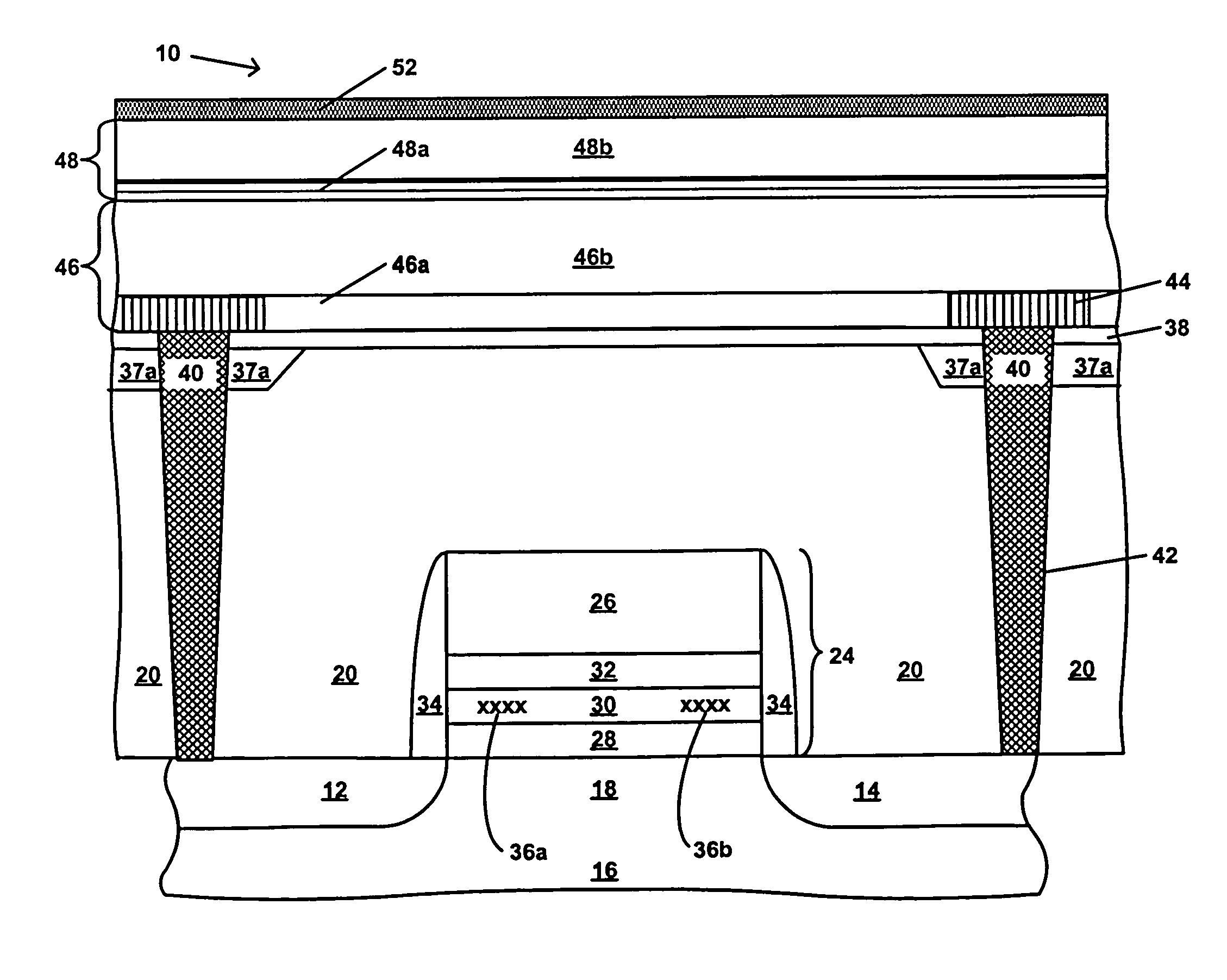
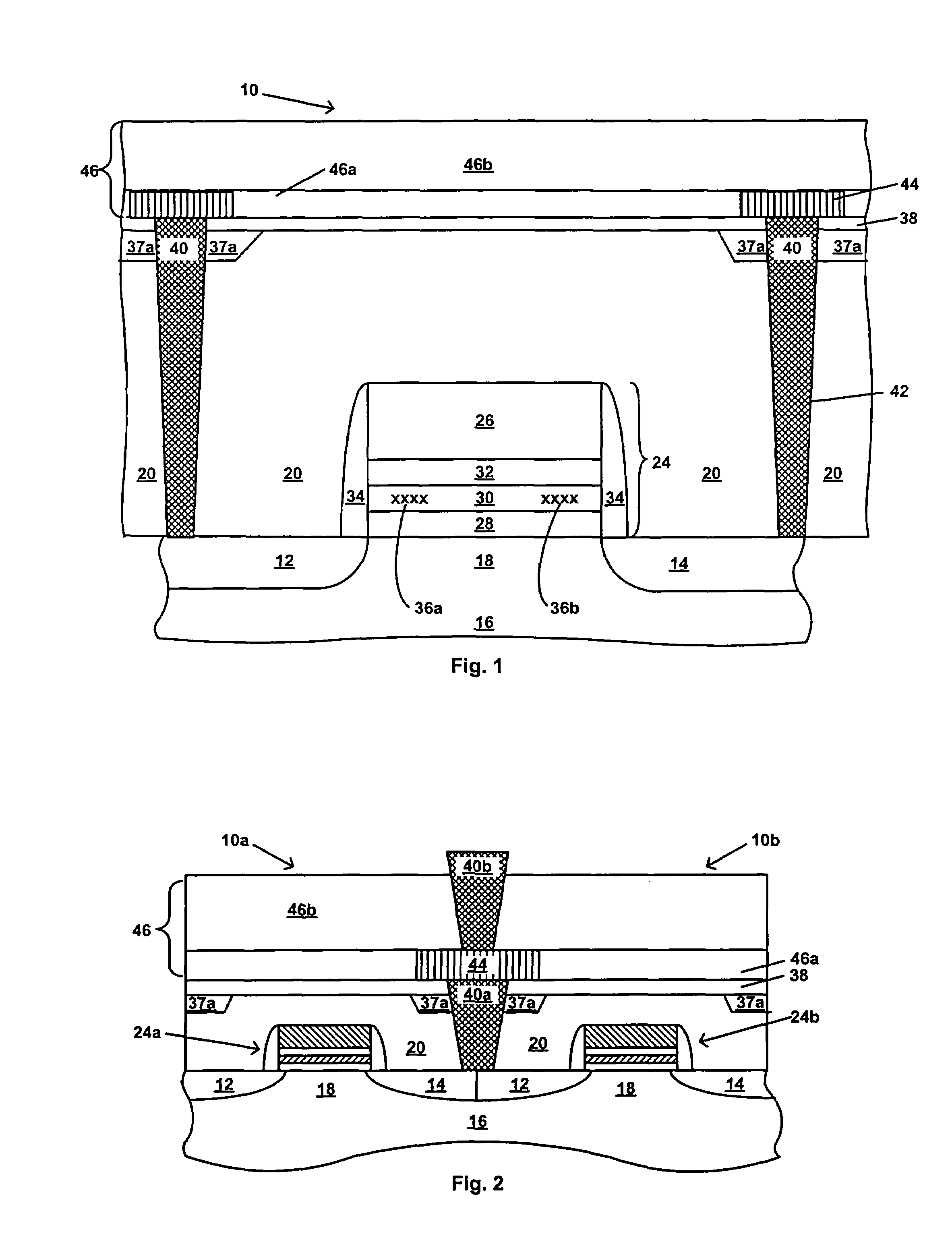
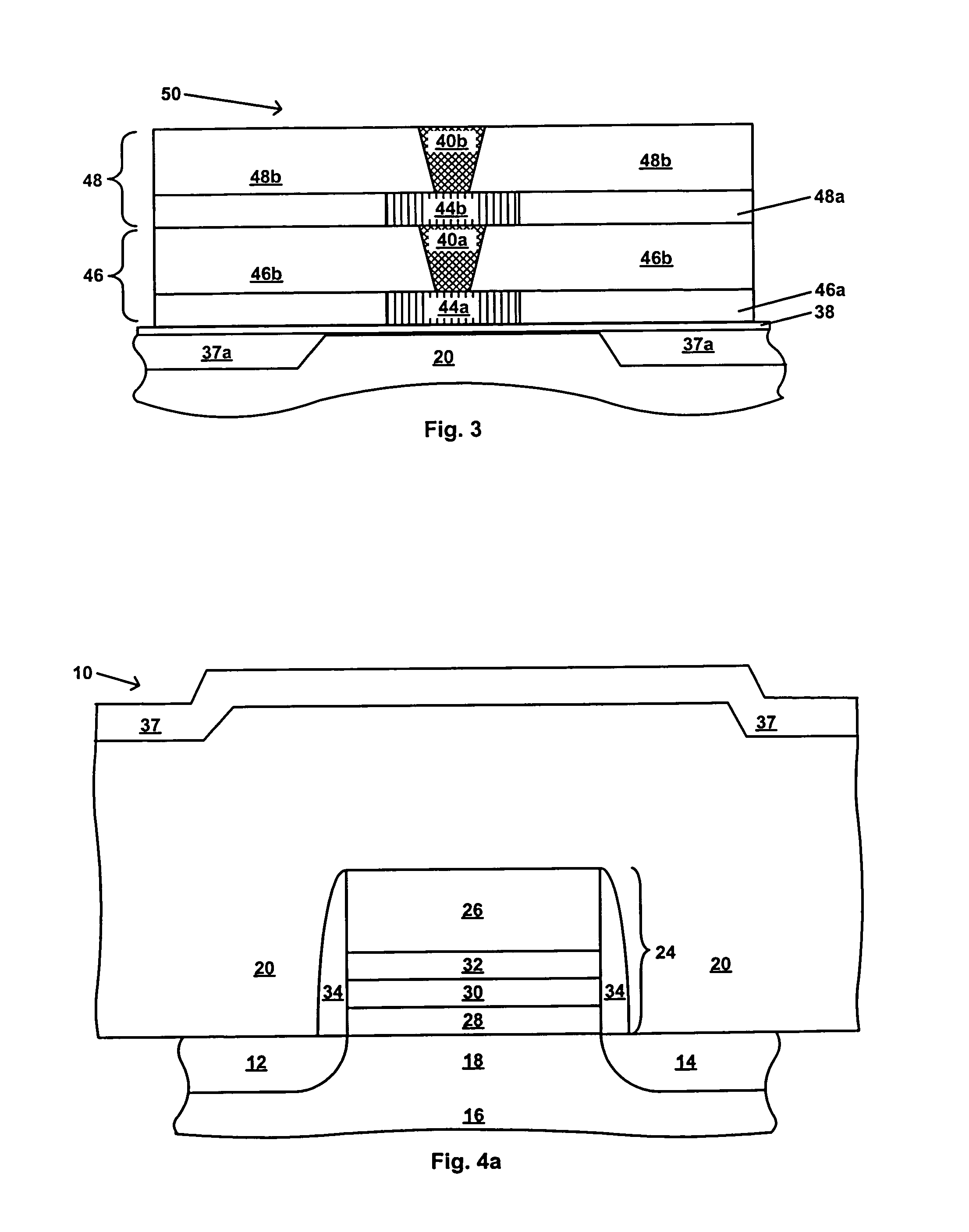
[0025]Referring first to FIG. 1, there is schematically shown in cross-section a transistor 10, which in one embodiment is a charge trapping dielectric flash memory cell, suitable for use in a dual-bit EEPROM device, such as the MIRRORBIT™. The transistor 10 includes source / drain regions 12 and 14 located in a semiconductor substrate 16 and separated by a channel region 18. The substrate 16 may be, for example, a single crystal silicon wafer. The substrate 16 may also be gallium arsenide, a silicon-on-insulator layer, an epitaxial layer, a silicon-germanium layer, a germanium-on-insulator layer, or other known semiconductor substrate. A stack gate 24 overlies the channel region 18. The stack gate 24 includes a control gate electrode 26, and an ONO structure including a bottom or tunnel oxide layer 28, a charge storage layer 30 and a top oxide layer 32, as shown in FIG. 1. In one embodiment, the charge storage layer 30 is a nitride containing charge storage layer. In one embodiment, ...


PUM


Abstract

A method of protecting a charge trapping dielectric flash memory cell from UV-induced charging, including fabricating a charge trapping dielectric flash memory cell in a semiconductor device; depositing and planarizing an interlevel dielectric layer over the charge trapping dielectric flash memory cell and depositing over the planarized interlevel dielectric layer at least one UV-protective layer, the UV-protective layer including a substantially UV-opaque material.

Description

TECHNICAL FIELD[0001]The present invention relates to a process for preparation of a charge trapping dielectric flash memory device including an improved contact integration and enhanced interlevel dielectric (ILD) chemical mechanical polishing (CMP) process and a device including such process in its fabrication.BACKGROUND ART[0002]Non-volatile memory devices are currently in widespread use in electronic components that require the retention of information when electrical power is terminated. Non-volatile memory devices include read-only-memory (ROM), programmable-read-only memory (PROM), erasable-programmable-read-only memory (EPROM), and electrically-erasable-programmable-read-only-memory (EEPROM) devices. EEPROM devices differ from other non-volatile memory devices in that they can be electrically programmed and erased. Flash EEPROM devices are similar to EEPROM devices in that memory cells can be programmed and erased electrically. However, flash EEPROM devices enable the erasin...

Claims


Application Information

Patent Timeline
IPC IPC(8): H01L29/788
CPCH01L23/53295H01L23/552H01L29/66833H01L29/7923H01L2924/0002H01L2924/00
Inventor ACHUTHAN, KRISHNASHREECHEUNG, PATRICK K.TABERY, CYRUSYANG, JEAN Y.CHENG, NINGNGO, MINH VAN
Owner INFINEON TECH LLC
Why Eureka
Try Eureka