Manufacturing method of semiconductor device, semiconductor manufacturing apparatus, plasma nitridation method, computer recording medium, and program

a manufacturing method and semiconductor technology, applied in semiconductor devices, electrical devices, capacitors, etc., can solve the problems of difficult formation of uniform nitride films, higher aspect ratios, and greater differences in nitridation degree among portions of trenches, so as to improve the nitridation reaction probability of subsequently supplied radicals, eliminate the variation in the thickness of formed nitride films, and improve the uniform thickness of nitride films

Inactive Publication Date: 2009-04-28
TOKYO ELECTRON LTD
View PDF17 Cites 9 Cited by
  • Summary
  • Abstract
  • Description
  • Claims
  • Application Information

AI Technical Summary

Benefits of technology

[0017]In each of the aspects of the present invention, if the lower electrode is made of polysilicon, nitriding its surface improves oxidation resistance at the time of heat treatment in a post process. Generally, since the capacity of a capacitor is large in a DRAM, applying the present invention to a capacitor of a DRAM makes the effect more prominent.
[0018]Further, if titanium nitride is used as the lower electrode, a surface of the titanium nitride is further nitrided, so that a nitrogen-rich layer is formed. This improves oxidation resistance at the time of heat treatment in a post process, similarly to the case of the polysilicon lower electrode.
[0020]In the present invention, nitridation processing is applied to a surface of a lower electrode of a capacitor, so that not only oxidation resistance is improved but also leakage current in the capacitor is reduced. As a result, an apparent dielectric constant is prevented from lowering and the thickness of an insulating film is allowed to be thick.
[0024]According to the plasma nitridation method of the present invention, in particular, even in a case of the shape having the recessed portion with a high aspect ratio, it is possible to eliminate variation in thickness of the formed nitride film to improve uniformity in thickness of the nitride film in a semiconductor wafer surface. Further, by controlling the process pressure by a RLSA-type plasma processing apparatus, it is possible to control a ratio of active species in the plasma, for example, radicals and ions. For example, on a high-pressure side, an ion ratio is low and a radical ratio is high. That is, it can be thought that on the high-pressure side, high-density radicals are generated, and thus the radicals being the active species can reach bottoms of the recessed portions to realize uniform nitridation of the whole recessed portions. When the radicals once collide with walls in the recessed portions such as trench holes and the nitride film is formed, a nitridation reaction probability of subsequently supplied radicals gets lower in surface portions of the nitride film, and the radicals can be made to reach the bottoms of the recessed portions by high pressure and the supply of a large amount of the radicals. Thus, on the high pressure side, plasma ion energy moderately works because it is damped. This makes it possible to form a uniform nitride film even in the recessed portion with a high aspect ratio while reducing damage to a film and a substrate.
[0025]Further, in a case where a target of the plasma nitridation processing is a polysilicon film as a lower electrode of a MIS capacitor with a trench structure, if the nitridation processing is applied to its surface beforehand, the oxidation of the surface of the polysilicon electrode is inhibited at the time of annealing for reformation and crystallization of a high dielectric constant film (high-k film), resulting in improved oxidation resistance. Therefore, reduction in capacitance can be surely prevented, so that it is possible to provide a semiconductor device such as a DRAM superior in electric property.

Problems solved by technology

However, the plasma processing disclosed in Japanese Patent Application Laid-open No. 2004-214655 has a unique problem of its own that it is difficult to form a uniform nitride film, depending on the shape of silicon on a surface of a processing target.
However, there has been a problem that a higher aspect ratio of the trench causes a greater difference in nitridation degree among portions of the trench, for example, between an upper portion and a lower portion (near a bottom of the trench), when a polysilicon electrode is plasma-nitrided in the course of manufacturing a MIS capacitor with the trench structure.
A possible cause of this problem may be that nitrogen radicals and nitrogen ions which are active species become inactive before reaching the bottom of the trench with the high aspect ratio.

Method used


Image

  • Manufacturing method of semiconductor device, semiconductor manufacturing apparatus, plasma nitridation method, computer recording medium, and program
  • Manufacturing method of semiconductor device, semiconductor manufacturing apparatus, plasma nitridation method, computer recording medium, and program
  • Manufacturing method of semiconductor device, semiconductor manufacturing apparatus, plasma nitridation method, computer recording medium, and program

Examples


Embodiment Construction

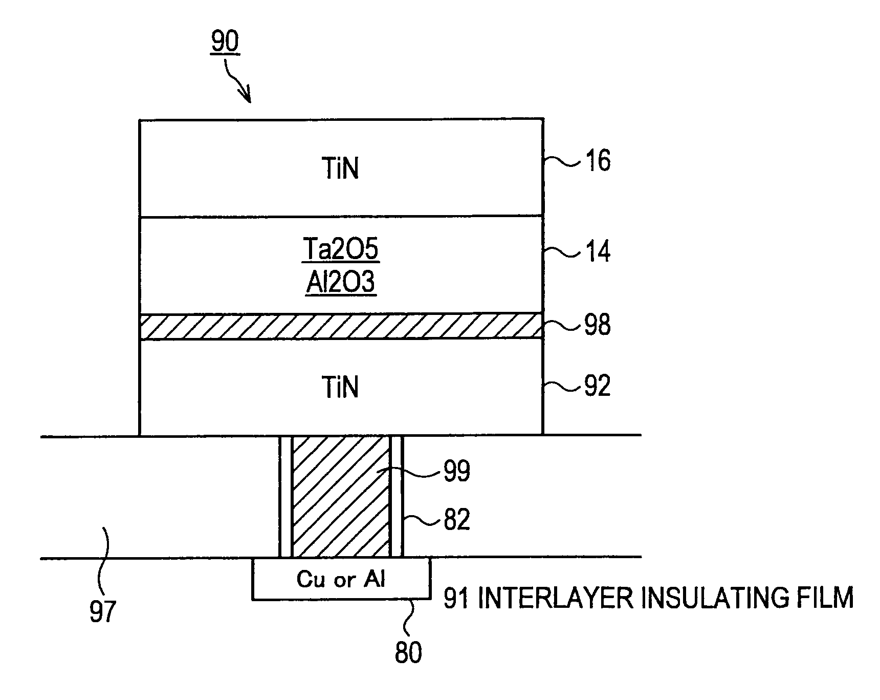
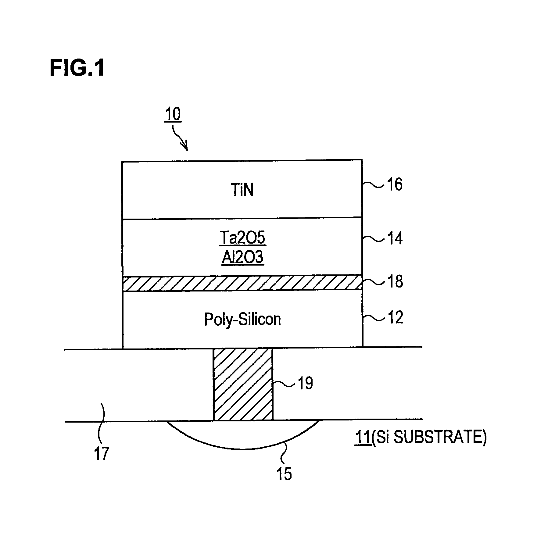
[0048]Hereinafter, the present invention will be described, taking manufacture of a capacitor in a DRAM as an example. Each of a plurality memory cells forming the DRAM has a structure including one MOS transistor, one capacitor, and element isolating regions. The MOS transistor includes, for example, N-doped source electrode and drain electrode on a P-type silicon substrate, a gate insulating film, and a gate electrode. The drain electrode is connected to a bit line. The gate electrode is connected to a word line. A protective oxide film is formed around the gate electrode portion.

[0049]FIG. 1 shows a structure of a capacitor 10 according to a first embodiment. The capacitor 10 includes an interlayer insulating film 17 formed on a silicon substrate 11, a lower electrode 12 formed on the interlayer insulating film 17, an insulating film 14 formed on the lower electrode 12, and an upper electrode layer 16 formed on the insulating film 14. The upper electrode layer 16 is a metal layer...


PUM


Abstract

An object of the present invention is to prevent an increase in film thickness and inhibit a reduction in capacity of a capacitor. In a semiconductor device having a capacitor, the capacitor includes a lower electrode, an upper electrode, and an insulating film interposed between the lower electrode and the upper electrode. A surface of the lower electrode on an insulating layer side is nitrided. If the lower electrode is made of polysilicon, nitriding the surface thereof increases oxidation resistance at the time of heat treatment in a post process. Particularly in a DRAM, the capacity of the capacitor is large, and therefore, this effect is significant. Further, leakage current inside the capacitor is also reduced.

Description

[0001]This is a continuation in part of PCT Application No. PCT / JP2004 / 013823, file on Sep. 22, 2004, which claims the benefit of a Japanese Patent Application No. 2003-334479, filed on Sep. 26, 2003, all of which are incorporated herein by reference.BACKGROUND OF THE INVENTION[0002]1. Field of the Invention[0003]The present invention relates to a manufacturing method of a semiconductor device, a semiconductor manufacturing apparatus, a plasma nitridation method, a computer recording medium, and a program.[0004]2. Description of the Related Art[0005]A DRAM as a semiconductor device has, in its memory cell, a MOS transistor and a capacitor storing charges for memory. In recent years, in accordance with the miniaturization of a semiconductor device, size shrinkage of the transistor and the capacitor in the semiconductor device is being demanded. Since the capacity of a capacitor is proportional to its area and inversely proportional to its thickness, there is a limit to reduction in t...

Claims


Application Information

Patent Timeline
Patent Type & Authority Patents(United States)
IPC IPC(8): H01L21/469H01L21/26
CPCH01L21/318H01L28/60H01L27/10852H01L21/02252H01L21/02247H01L21/02186H10B12/033
Inventor SASAKI, MASARUKABE, YOSHIRO
Owner TOKYO ELECTRON LTD
Why Eureka
Try Eureka