Method for correcting systematic errors in a laser processing system

Active Publication Date: 2006-08-17
ELECTRO SCI IND INC
View PDF4 Cites 17 Cited by
  • Summary
  • Abstract
  • Description
  • Claims
  • Application Information

AI Technical Summary

Benefits of technology

[0013] The advantages of this method of estimating Z axis error are that it is more accurate than previous methods, and since substantial portions of the error can be pre-computed and stored, it is faster than previous methods. These are desirable features of a l

Problems solved by technology

While these calculations are mathematically possible, they are mor

Method used


Image

  • Method for correcting systematic errors in a laser processing system
  • Method for correcting systematic errors in a laser processing system
  • Method for correcting systematic errors in a laser processing system

Examples


Embodiment Construction

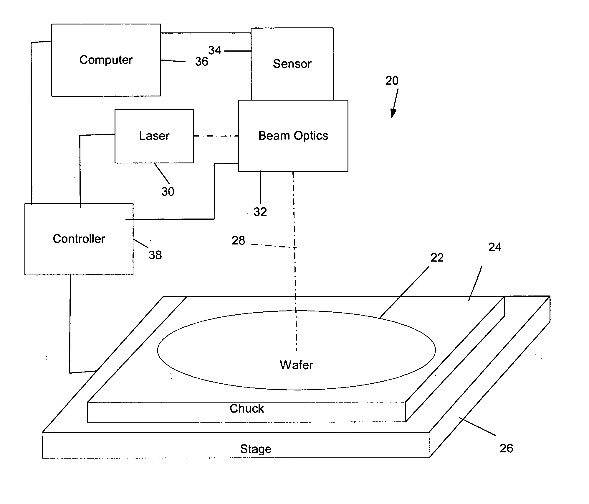
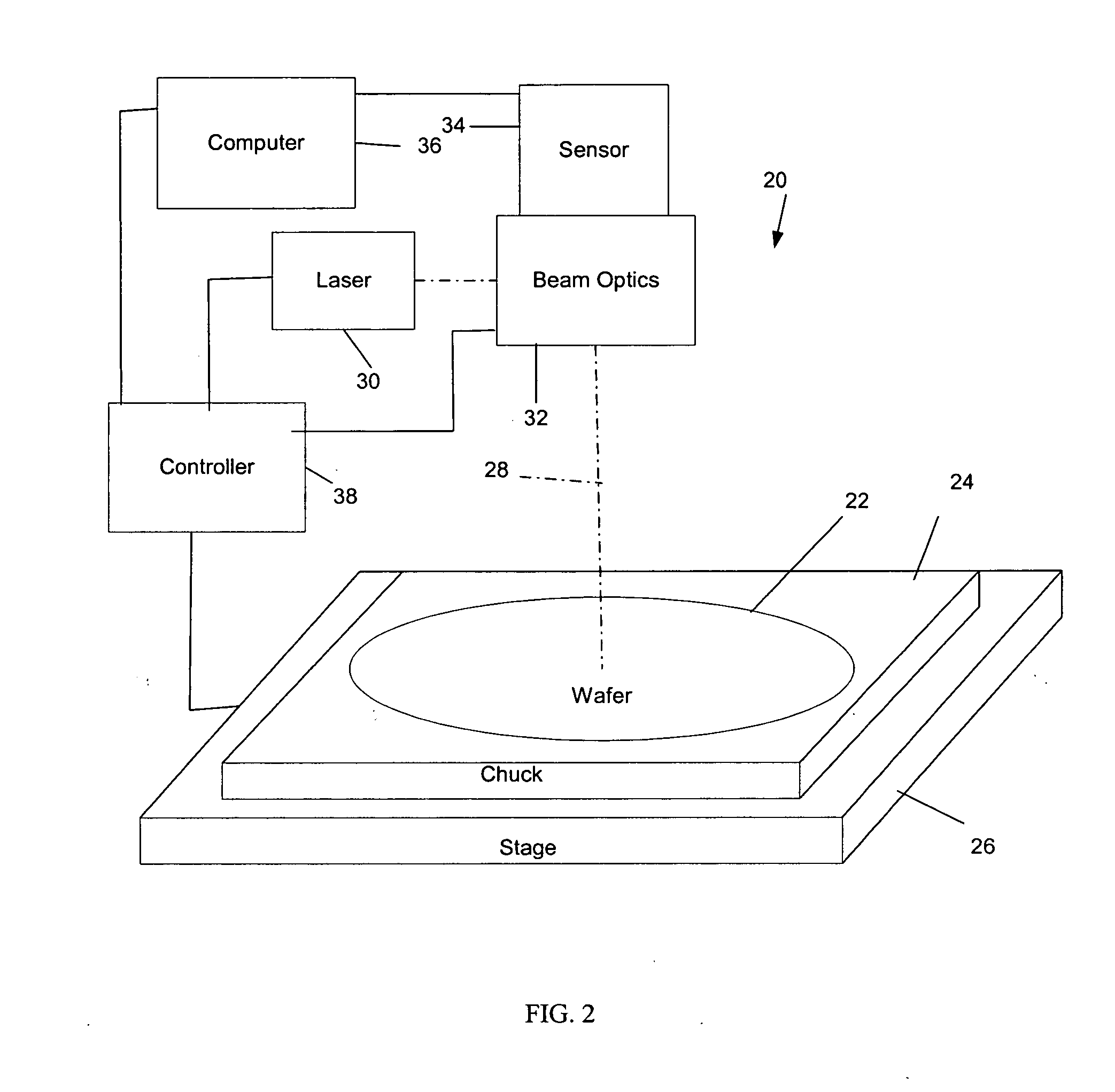
[0025] In a preferred embodiment, a silicon wafer is fixed in place in a chuck and positioned with respect to a laser beam that will be pulsed for incidence on micromachine fusible links on the surface of the wafer. In this case, several factors can cause variations in the X, Y, and Z accuracy of a laser micromachining system. Accuracy is a function of the relationship between the laser beam and the workpiece. The relationship between the laser beam and the workpiece is a function of several moving parts, optics, and the workpiece, each with its own sources of error. For instance, in a preferred embodiment, the wafer chuck may be attached to an X, Y table that moves the wafer under the laser beam to position it at a desired location on the wafer. Alignment of the X and Y axes to each other and alignment of the plane formed by the X and Y axes, in addition to possible errors in travel along each axis, all contribute to errors attributable to the chuck motion control, among other poss...


PUM

PropertyMeasurementUnit
Sizeaaaaaaaaaa
Densityaaaaaaaaaa
Bending strengthaaaaaaaaaa

Abstract

A method for calibrating a laser micro-machining system in three dimensions includes scanning a sample workpiece to determine the 3D surface, calculating the best fit surfaces to the scanned data in a series of steps, and storing the results so that subsequent workpieces can be calibrated to remove systematic errors introduced by variations in an associated material handling subsystem. The method optionally uses plate bending theory to model particulate contamination and splines to fit the 3D surface in a piecewise fashion to minimize the effect of local variations on the entire surface fit.

Description

TECHNICAL FIELD [0001] This invention relates to calibration of material handling systems and more particularly to methods for calibrating material handling systems that fix in place workpieces such as semiconductor wafers for laser processing operations. This invention provides methods for identifying and correcting systematic errors that can be pre-computed and applied to each subsequent workpiece processed by the system. BACKGROUND OF THE INVENTION [0002] Laser micro-machining is employed in a variety of operations related to semiconductor and electronics manufacturing. Some of the applications of laser processing include repair, configuration, and marking semiconductor die such as dynamic random access memory (DRAM); laser trimming of passive components; drilling vias in substrates; and impedance tuning of integrated semiconductor devices. In the example of DRAM repair, a semiconductor wafer containing DRAM integrated circuits (ICs) is tested and a list is prepared of those memo...

Claims


Application Information

Patent Timeline
IPC IPC(8): B23K26/03G06F19/00
CPCB23K26/04B23K2201/40B23K2101/40G16Z99/00H01L21/302H01L21/82H01L22/00
Inventor SWARINGEN, STEPHEN NEALBRULAND, KELLYWELLS, ANDREW
Owner ELECTRO SCI IND INC
Why Eureka
Try Eureka