Thin film resistor with current density enhancing layer (CDEL)

a thin film resistor and density enhancement technology, applied in resistor details, resistors, transistors, etc., can solve the problems of insufficient protection (and capping) of sin or sicn, ineffective prevention of resistance shifting, and prior art resistors comprised of doped polysilicon can only provide limited resistance within a limited space, so as to enhance the current carrying capability of the resistor, enhance the current carrying capability, and improve the adhesion

Active Publication Date: 2006-08-17
GLOBALFOUNDRIES US INC
View PDF17 Cites 42 Cited by
  • Summary
  • Abstract
  • Description
  • Claims
  • Application Information

AI Technical Summary

Benefits of technology

[0016] It is a further object to provide a novel thin film resistor structure and method of fabricating the resistor by providing a barrier material over the thin-film resistor structure to thereby enhance the current-carrying capability of the resistor.
[0017] It is another object of the present invention to provide a novel thin film resistor structure of TaN material having an added barrier material layer with better adhesion to TaN to enhance the current carrying capability of the resistor.
[0018] According to the invention, this added barrier material is called the Current Density Enhancement Layer (CDEL) and provides increased re...

Problems solved by technology

However, due to the properties of polysilicon, a prior art resistor comprised of doped polysilicon can only provide a limited resistance within a limited space.
Employing a polysilicon resistor to provide relatively high resistance then becomes a problem in designing and fabricating a highly integrated semiconductor device.
It is suspected, how...

Method used


Image

  • Thin film resistor with current density enhancing layer (CDEL)
  • Thin film resistor with current density enhancing layer (CDEL)
  • Thin film resistor with current density enhancing layer (CDEL)

Examples


Embodiment Construction

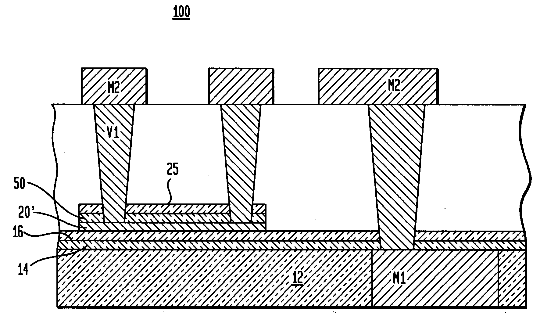
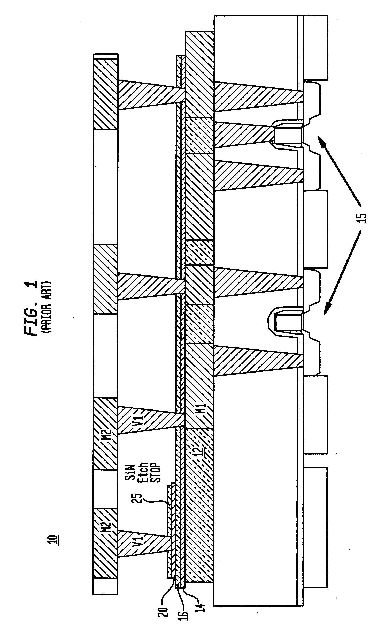
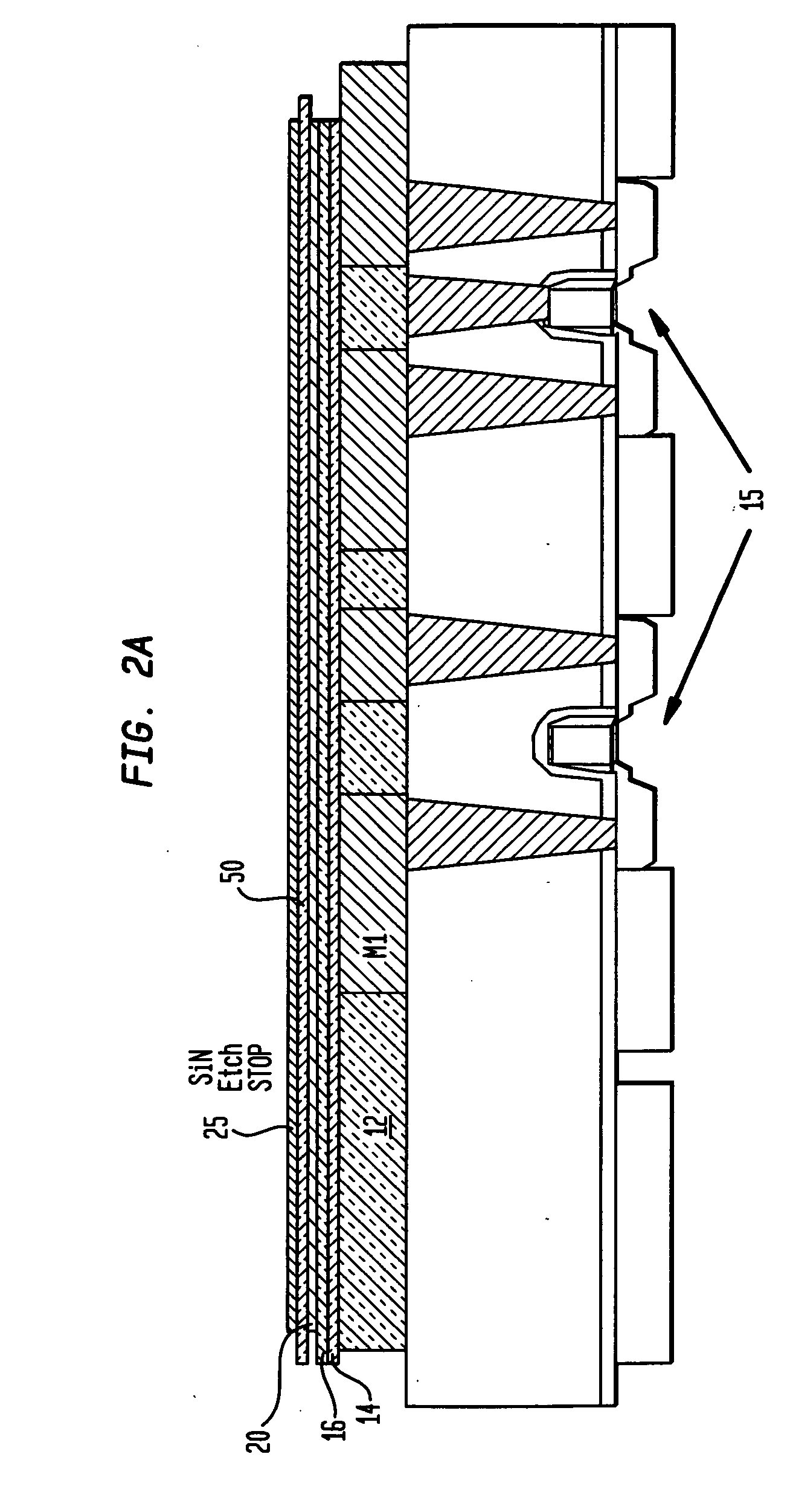
[0025] The present invention, which provides processes for fabricating a precision thin-film resistor that exhibits enhanced current carrying capability, will now be described in greater detail by referring to the various drawings that accompany the present application. The drawings are provided herein for illustrative purposes and thus they are not drawn to scale.

[0026] Moreover, the drawings of the present invention show a fragment of a semiconductor wafer or chip in which only one resistor device region is shown in a Back-End-Of-Line (BEOL) manufacturing process. Although the drawings show the presence of only a single resistor device region, the present processes can be used in forming a plurality of resistors across different resistor device regions on the surface of a single semiconductor chip or wafer. Moreover, the invention is applicable to front-end-of-line (FEOL) processes whereby the inventive resistor device structure is formed on a Si-containing substrate, for instanc...


PUM


Abstract

A thin film resistor device and method of manufacture includes a layer of a thin film conductor material and a current density enhancing layer (CDEL). The CDEL is an insulator material adapted to adhere to the thin film conductor material and enables the said thin film resistor to carry higher current densities with reduced shift in resistance. In one embodiment, the thin film resistor device includes a single CDEL layer formed on one side (atop or underneath) the thin film conductor material. In a second embodiment, two CDEL layers are formed on both sides (atop and underneath) of the thin film conductor material. The resistor device may be manufactured as part of both BEOL and FEOL processes.

Description

BACKGROUND [0001] 1. Field of the Invention [0002] The present invention relates generally to the field of semiconductor thin film resistors, and more particularly, to a novel integrated circuit thin film resistor having a current density enhancing layer. [0003] 2. Description of the Prior Art [0004] In semiconductor integrated circuits (ICs), a resistor may be used to control the resistance of other electronic components of the IC. As is known to those skilled in the art, the resistance, R, of a resistor is proportional to the length, L, of the resistor and the reciprocal cross sectional area, 1 / A, of the resistor; the L and A are measured in the direction of current flow. The basic equation for resistance of a resistor is thus: R=L / A, where R, L and A are as defined above. [0005] Prior art resistors are typically composed of polysilicon that has been doped. As the integration of semiconductor devices increases, each component within a semiconductor IC has to provide equivalent or...

Claims


Application Information

Patent Timeline
IPC IPC(8): H01C1/012
CPCH01C7/006H01L23/5228H01L27/0629H01L27/0688H01L28/24H01L2924/0002H01L2924/00
Inventor CHINTHAKINDI, ANIL K.ESHUN, EBENEZER E.
Owner GLOBALFOUNDRIES US INC
Why Eureka
Try Eureka