Inspection method and inspection apparatus using charged particle beam

a technology of charged particle beam and inspection apparatus, which is applied in the direction of discharge tube/lamp details, material analysis using wave/particle radiation, nuclear engineering, etc., can solve the problems of low shadow contrast, low sensitivity, and inability to emphasize contrast, and achieve high sensitivity. , the effect of high sensitivity

Inactive Publication Date: 2006-08-24
HITACHI HIGH-TECH CORP
View PDF1 Cites 35 Cited by
  • Summary
  • Abstract
  • Description
  • Claims
  • Application Information

AI Technical Summary

Benefits of technology

[0012] According to the present invention, it is possible to obtain an image with emphasized shadow contrast during the inspection of a semiconductor device and the like having circuit patterns, and thereby detect shal

Problems solved by technology

In JP-A No.273569/1997, however, all the elevation angle components (0 to 90 degrees) are detected for emitted secondary electrons, and consequently the shadow contrast lowers, making it impossible to emphasize the contrast.
For shallow asperities, the shadow contrast is low and defect detection may fail.
However, if the detector plates are not disposed symmetrica

Method used


Image

  • Inspection method and inspection apparatus using charged particle beam
  • Inspection method and inspection apparatus using charged particle beam
  • Inspection method and inspection apparatus using charged particle beam

Examples


first embodiment

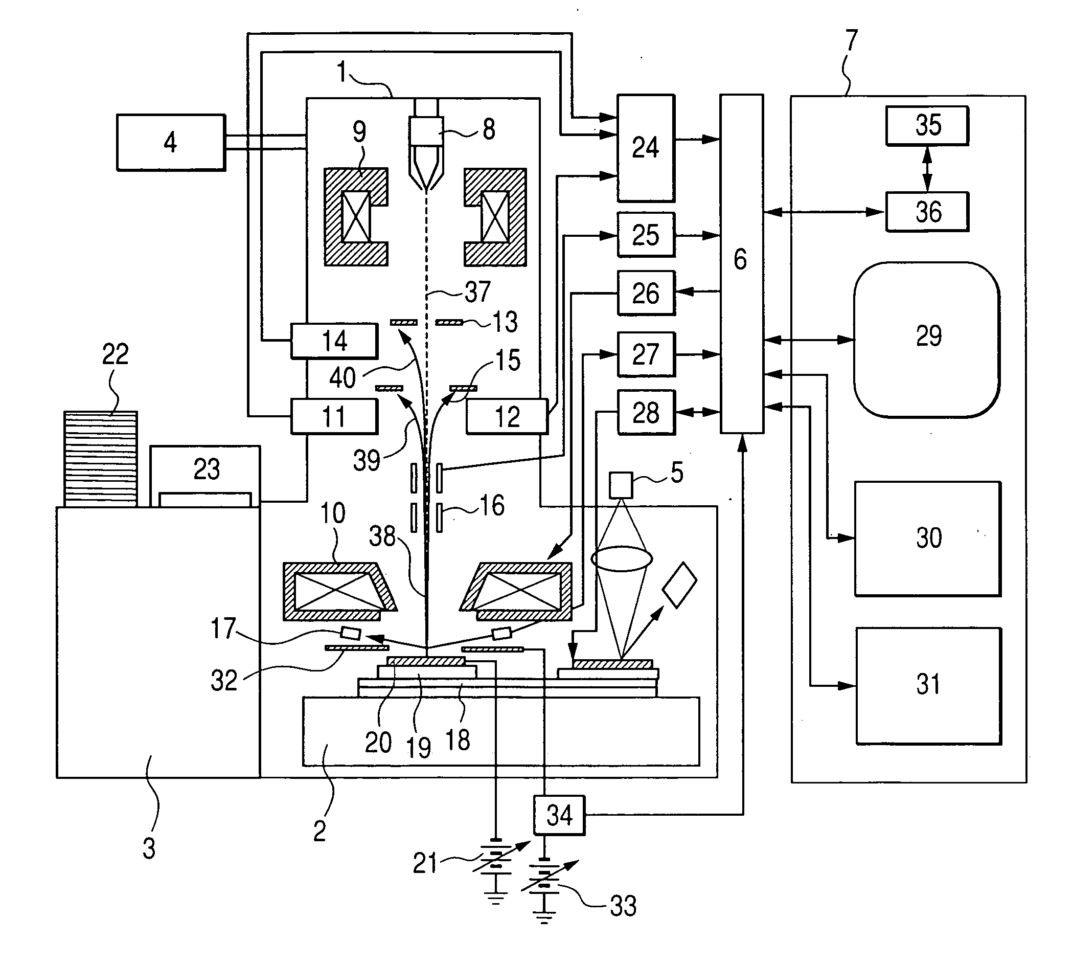
[0031] In this embodiment, an example of defect classification using a review SEM. FIG. 1 shows an example configuration of a review SEM. This apparatus comprises an electro-optic system 1, a stage mechanism system 2, a wafer carrying system 3, an evacuation system 4, an optical microscope 5, a control system 6, and an operation unit 7.

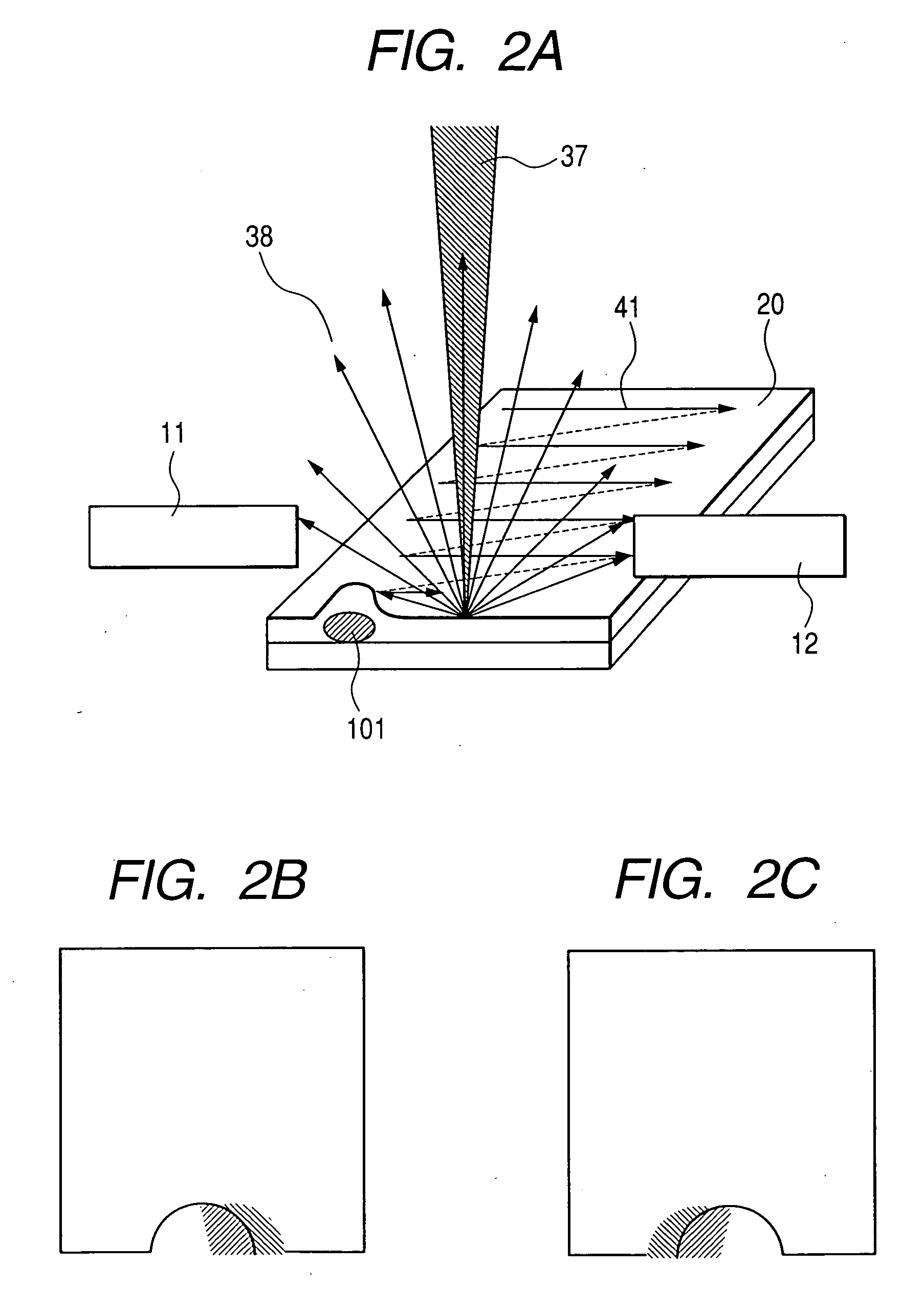
[0032] The electro-optic system is composed of an electron source 8, a condenser lens 9, an objective lens 10, a first detector plate 11, a second detector plate 12, a first reflector plate 13, a third detector plate 14, a second reflector plate 15, a deflector 16, a wafer height detector 17, an electrode 32 disposed opposite to the stage, an electrode power supply 33, and an electrode power supply control unit 34.

[0033] The stage mechanism system 2 includes an XY stage 18, a holder 19 to hold a wafer as a specimen, and a retarding power supply 21 to apply a negative voltage to the holder 19 and wafer 20. To the XY stage 18 is attached a position de...

second embodiment

[0046] Now, a second embodiment is described. FIG. 8 shows the configuration of the second embodiment. In this embodiment, a so-called ExB deflector 201 for deflecting secondary electrons is disposed on the light axis of a primary electron beam. The other configuration is the same as that of the first embodiment. The term ExB deflector here is a deflector overlapping electric field and magnetic field, wherein, for the primary electron beam, the amount of deflection by electric field and that of magnetic field are set so that they become the same in opposite direction from each other to cancel out the deflection effect of each field, and, electric field and magnetic field acts on secondary electrons in such a direction in which the amount of deflection by electric field becomes equal to that of magnetic field, to thereby deflect only the secondary electrons independently.

[0047]FIG. 9 shows the operation of the second embodiment. The central trajectory 202 of secondary electrons is d...

third embodiment

[0052] Now, a third embodiment is described. The entire configuration is similar to that of the second embodiment shown in FIG. 8. In this embodiment, the ExB deflector is composed of a 4-polar electrode and a magnetic pole, and secondary electrons can be deflected at any azimuth. As a result, it is possible to align the secondary electrons not only in the direction (x direction in FIG. 9) of separating the reflector plate 15 as shown in FIG. 9, but also in the direction (y direction) perpendicular to the surface of the page on which FIG. 9 is drawn. This allows correction of a displacement in the y direction of the central trajectory of secondary electrons relative to the opening of the reflector plate 15. It is also possible to adjust so that secondary electrons impinge on the reflector plate in a desired manner.


PUM


Abstract

To establish a technique that enables sorting of the elevation and azimuth angle in the direction of emitting secondary electrons and obtaining images with emphasized contrast, in order to perform the review and analysis of shallow asperities and microscopic foreign particles in a wafer inspection during the manufacture of semiconductor devices, an electromagnetic overlapping objective lens is used to achieve high resolution, an electron beam is narrowly focused using the objective lens, an electric field for accelerating secondary electrons in the vicinity of a wafer in order to suppress the dependence on secondary electron energy of the rotation of secondary electrons generated by irradiation of the electron beam, a ring-shaped detector plate is disposed between an electron source and the objective lens, and the low angle components of the elevation angle of the secondary electrons, as viewed from the place of generation, and the high angle components are separated and also the azimuth components are separated and detected.

Description

CLAIM OF PRIORITY [0001] The present application claims priority from Japanese application JP 2005-041531 filed on Feb. 18, 2005, the content of which is hereby incorporated by reference into this application. FIELD OF THE INVENTION [0002] The present invention relates to a manufacturing method and apparatus for substrates having microscopic circuit patterns, such as semiconductor devices and liquid crystal devices, and more specifically to the pattern inspection technology for semiconductor devices and photomasks. Further specifically, the present invention relates to a review SEM whereby, after an optical imaging based or electron beam based defect inspection of an arbitrary area on an unfinished wafer during the manufacturing process of semiconductor devices, a defect review is performed with high resolutions based on the defect coordinate. BACKGROUND OF THE INVENTION [0003] A semiconductor device is manufactured by repeating a process of transferring patterns formed with photoma...

Claims


Application Information

Patent Timeline
IPC IPC(8): G21G5/00
CPCH01J37/244H01J37/28H01J2237/24495H01J2237/2817
Inventor NISHIYAMA, HIDETOSHIFUKUDA, MUNEYUKITAKAHASHI, NORITSUGUSATO, MITSUGUFUKADA, ATSUKOSUZUKI, NAOMASA
Owner HITACHI HIGH-TECH CORP
Why Eureka
Try Eureka