

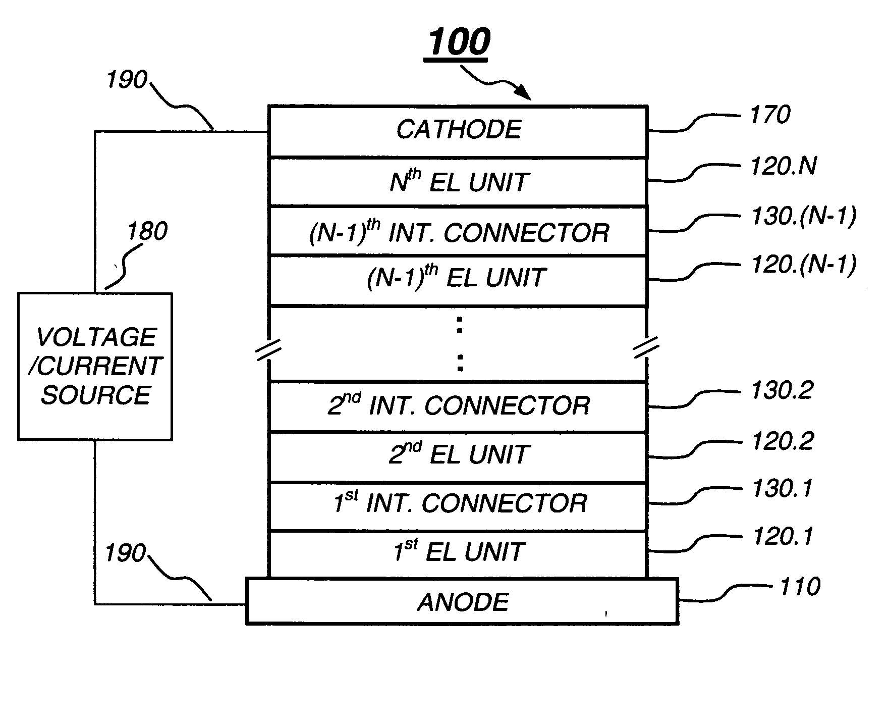
Tandem OLED having an organic intermediate connector
a technology of organic intermediate connectors and oleds, which is applied in the direction of discharge tube luminescnet screens, natural mineral layered products, other domestic articles, etc., can solve the problems of high cost, high manufacturing complexity, and short operational life, and achieve the effect of simple fabrication and low cos
- Summary
- Abstract
- Description
- Claims
- Application Information
AI Technical Summary
Benefits of technology
Problems solved by technology
Method used
Image

Examples
example 1
Comparative
[0130] The preparation of a conventional OLED is as follows:
[0131] A ˜1.1 mm thick glass substrate coated with a transparent indium-tin-oxide (ITO) conductive layer was cleaned and dried using a commercial glass scrubber tool. The thickness of ITO is about 42 nm and the sheet resistance of the ITO is about 68 Ω / square. The ITO surface was subsequently treated with oxidative plasma to condition the surface as an anode. A layer of CFx, 1 nm thick, was deposited on the clean ITO surface as the hole-injecting layer by decomposing CHF3 gas in an RF plasma treatment chamber. The substrate was then transferred into a vacuum deposition chamber for deposition of all other layers on top of the substrate. The following layers were deposited in the following sequence by evaporation from a heated boat under a vacuum of approximately 10−6 Torr:
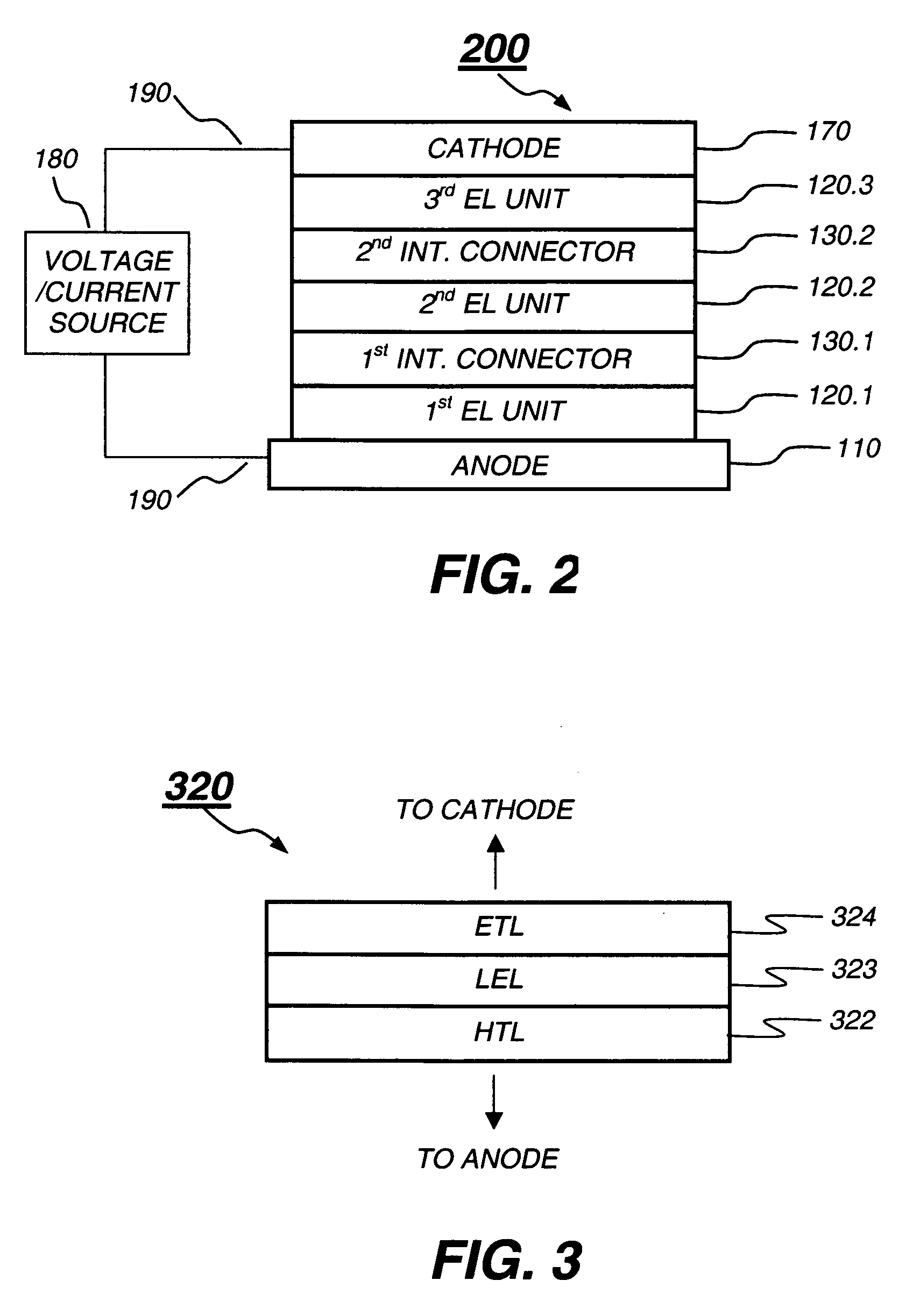
1. EL Unit:
[0132] a) an HTL, 100 nm thick, including “4,4′-bis[N-(l-naphthyl)-N-phenylamino]biphenyl” (NPB);
[0133] b) a LEL, 20 nm thick, ...
example 2
Comparative
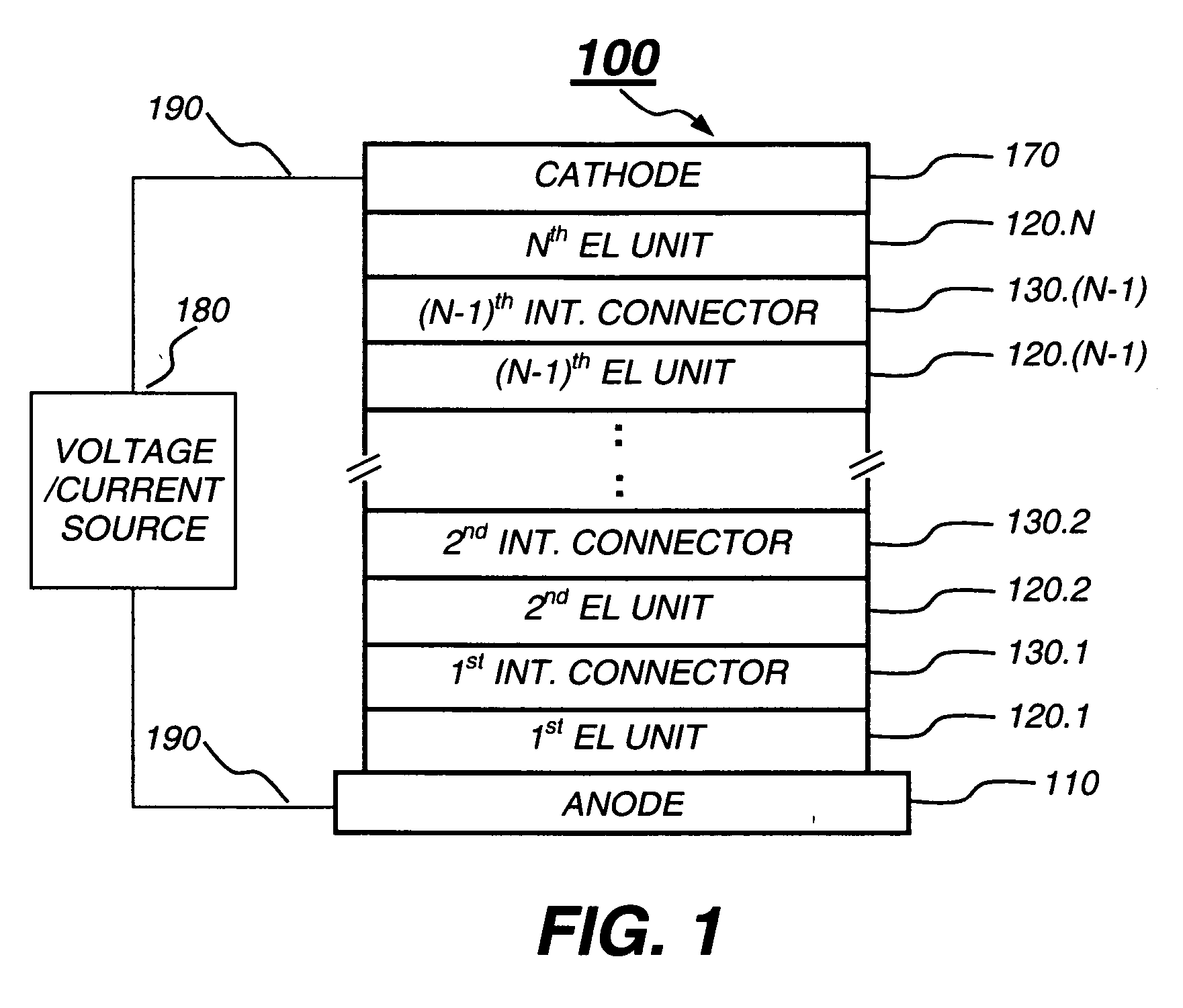
[0137] A tandem OLED was constructed with the similar fabrication methods to those used in Example 1, and the deposited layer structure is:
1. 1st EL Unit:
[0138]
[0139] The 1st EL unit is the same as the EL unit in Example 1.
2. 2nd EL Unit:
[0140] The 2nd EL unit is the same as the EL unit in Example 1 except that the thickness of the HTL (NPB layer) is changed from 100 nm to 85 nm.
3. Cathode: approximately 210 nm thick, including MgAg.
[0141] This tandem OLED requires a drive voltage of about 38.5 V to pass 20 mA / cm2. Under this test condition, the device has a luminance of 1410 cd / m2, and a luminous efficiency of about 7.1 cd / A. Its CIEx and CIEy are 0.282, 0.660, respectively, with an emission peak at 524 nm. The EL performance data are summarized in Table 1.
[0142] Since there is no intermediate connector between the two EL units, the EL performance of the tandem OLED is very poor requiring a drive voltage 5 times as high as that of the conventional OLED while e...
example 3
Comparative
[0143] Another tandem OLED was constructed with the similar fabrication methods to those used in Example 1, and the deposited layer structure is:
1. 1st EL Unit:
[0144] The 1st EL unit is the same as the EL unit in Example 1.
2. 1st Intermediate Connector:
[0145] a metal layer, 10 nm thick, including Ag.
3. 2nd EL Unit:
[0146] The 2nd EL unit is the same as the EL unit in Example 1 except that the thickness of the HTL (NPB layer) is changed from 100 nm to 75 nm.
4. Cathode: approximately 210 nm thick, including MgAg.
[0147] This tandem OLED requires a drive voltage of about 28.7 V to pass 20 mA / cm2. Under this test condition, the device has a luminance of 183 cd / m2, and a luminous efficiency of about 0.9 cd / A. Its CIEx and CIEy are 0.288, 0.654, respectively, with an emission peak at 524 nm. The EL performance data are summarized in Table 1.
[0148] Although there is an Ag layer as an intermediate connector between the two EL units, this intermediate connector is not ...
PUM
| Property | Measurement | Unit |
|---|---|---|
| Thickness | aaaaa | aaaaa |
| Thickness | aaaaa | aaaaa |
| Percent by volume | aaaaa | aaaaa |
Abstract
Description
Claims
Application Information