Body capacitor for SOI memory description

a silicon-on-insulator and memory device technology, applied in the field of body capacitors for soi memory devices, can solve the problems of increasing chip area, increasing dynamic power dissipation, slow performance, etc., and achieves the effect of effectively holding the body charge and minimizing the overlap capacitance of the body-capacitor

Inactive Publication Date: 2006-08-24
GLOBALFOUNDRIES INC
View PDF2 Cites 14 Cited by
  • Summary
  • Abstract
  • Description
  • Claims
  • Application Information

AI Technical Summary

Benefits of technology

[0005] The present invention provides a semiconductor structure having a body capacitor plate, which is formed with a process that assures that the body capacitor plate is self-aligned to both the source line (SL) diffusion and the bitline (BL) diffusion. Thus, the amount of overlap between the SL and the BL diffusions and the body capacitor plate is precisely controlled. Unlike the Toshiba cell, the inventive 1-T dynamic access memory (DRAM) cell minimizes the body-capacitor overlap capacitances among source and drain junctions and provides coupling nearly exclusively to the body regions to effectively hold the body charges.

Problems solved by technology

This increased bitline capacitance results in a combination of slower performance, increased chip area (because larger drivers are required to compensate for the larger parasitic capacitance), and increased dynamic power dissipation.

Method used


Image

  • Body capacitor for SOI memory description
  • Body capacitor for SOI memory description
  • Body capacitor for SOI memory description

Examples


Embodiment Construction

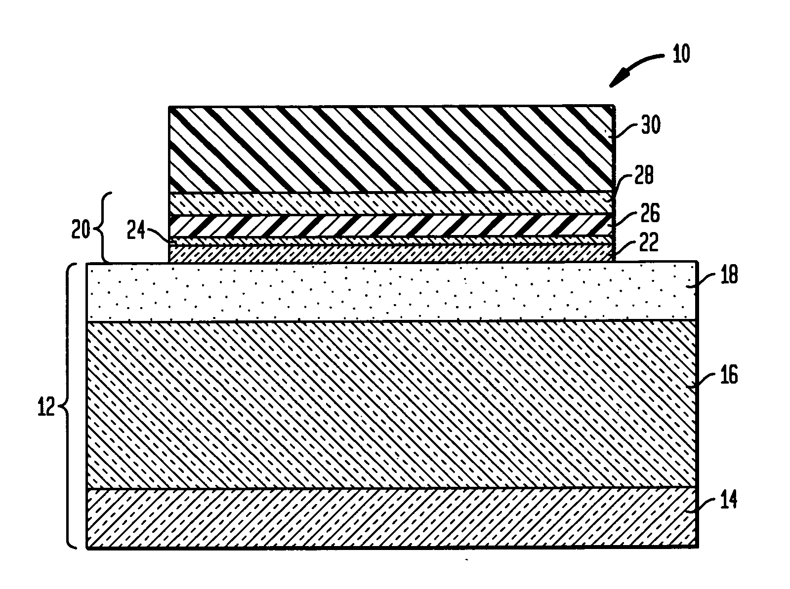
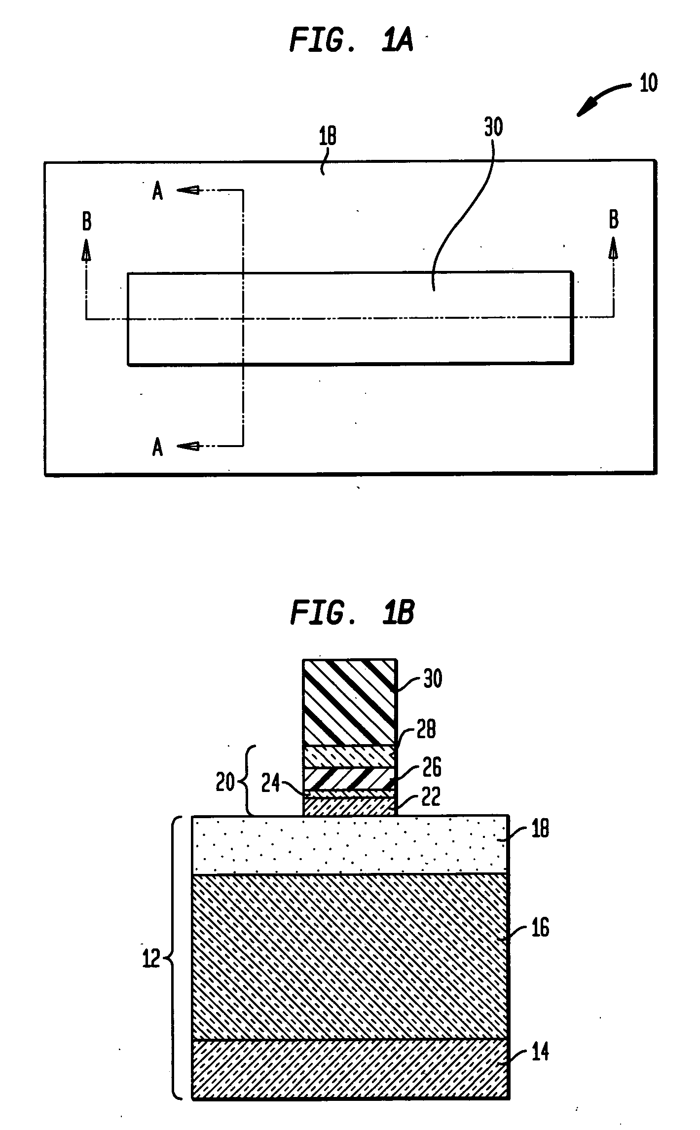
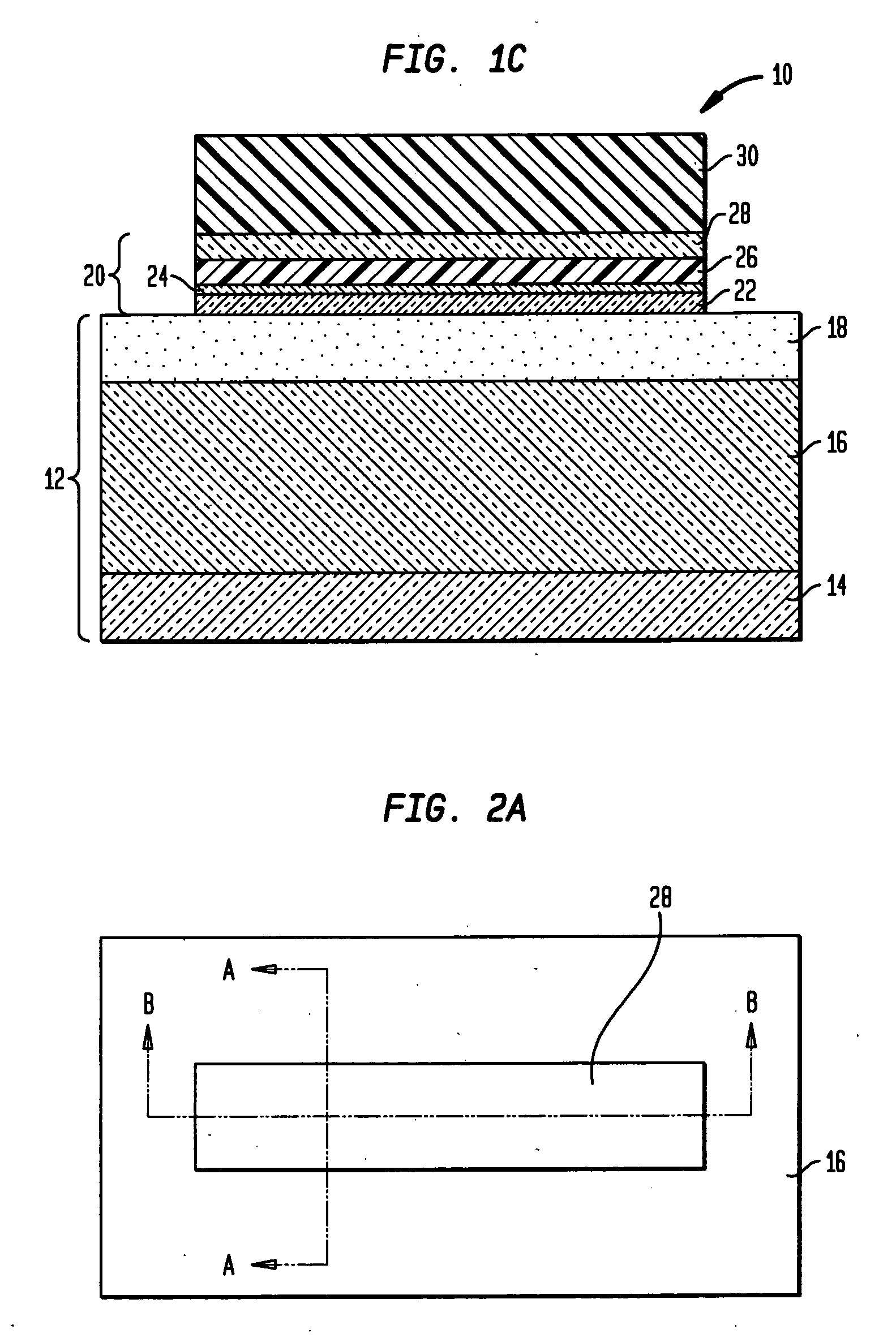
[0027] The present invention, which provides a self-aligned SOI body capacitor and a method of fabricating the same, will now be described in greater detail by referring to the drawings that accompany the present application. The drawings are provided herein for illustrative purposes and thus they are not drawn to scale.

[0028] In FIGS. 1-20, the structure through various processing steps is illustrated in different views. Drawing A represents a top-down view where cross-sections A-A and B-B, and in some instances C-C, are shown. Drawing B is a cross sectional view along the line A-A, Drawing C is a cross sectional view along the line B-B, and Drawing D is a cross sectional view along the line C-C. “A-A” is a cross section in a vertical cutting a plane parallel to a wordline location, and through the center of the wordline location. “B-B” is a cross section in a vertical cutting plane parallel to a bitline location, and through the center of the bitline location. “C-C” is a cross se...


PUM


Abstract

A semiconductor structure having a body capacitance plate, which is formed with a process that assures that the body capacitance plate is self-aligned to both the source line (SL) diffusion and the bitline diffusion is provided. Thus the amount of overlap between the SL and the bitline diffusions and the body capacitance plate is precisely controlled. More specifically, the present invention forms the structure of a 1T-capacitorless SOI body charge storage cell having sidewall capacitor plates using a process that assures that there is 1) minimal overlap between plate and source/drain diffusions, and 2) that the minimal overlap obtained in the present invention is precisely controlled and is not subject to alignment tolerances. The inventive cell results in larger signal margin, improved performance, smaller chip size, and reduced dynamic power dissipation relative to the prior art.

Description

FIELD OF THE INVENTION [0001] The present invention relates to a semiconductor structure and a method of fabricating the same. More particularly, the present invention relates to a body capacitor for a silicon-on-insulator (SOI) memory device. The present invention also provides a method for fabricating such a semiconductor structure in which the processing steps assure that there is minimal overlap capacitance between the capacitor plate and the source / drain diffusions that is controlled and is not subjected to alignment tolerances. The present invention also relates to a semiconductor memory cell layout that includes the inventive SOI body capacitor used in a folded bitline design. BACKGROUND OF THE INVENTION [0002] Several one transistor (1T)-capacitorless cells that store charge in the body of a silicon-on-insulator (SOI) metal oxide semiconductor field effect transistor (MOSFET) are known in the art. Both the Fazan cell (See, for example, IEEE Electron Device Letters, Vol. 23, ...

Claims


Application Information

Patent Timeline
Patent Type & Authority Applications(United States)
IPC IPC(8): H01L21/3205
CPCH01L21/84H01L27/108H01L27/10832H01L27/10858H01L27/1203H01L29/94H10B12/373H10B12/036H10B12/00
Inventor MANDELMAN, JACK A.HSU, LOUIS C.JOSHI, RAJIV VASANT
Owner GLOBALFOUNDRIES INC
Why Eureka
Try Eureka