Laser irradiation method and apparatus for forming a polycrystalline silicon film

a polycrystalline silicon and laser irradiation technology, applied in semiconductor/solid-state device testing/measurement, manufacturing tools, instruments, etc., can solve the problem of difficult evaluation and management of molten state, which should essentially be managed

Inactive Publication Date: 2006-08-31
VISTA PEAK VENTURES LLC
View PDF6 Cites 7 Cited by
  • Summary
  • Abstract
  • Description
  • Claims
  • Application Information

AI Technical Summary

Problems solved by technology

This is because the molten state which should essentially be managed is difficult to evaluate and manage.

Method used


Image

  • Laser irradiation method and apparatus for forming a polycrystalline silicon film
  • Laser irradiation method and apparatus for forming a polycrystalline silicon film
  • Laser irradiation method and apparatus for forming a polycrystalline silicon film

Examples


second embodiment

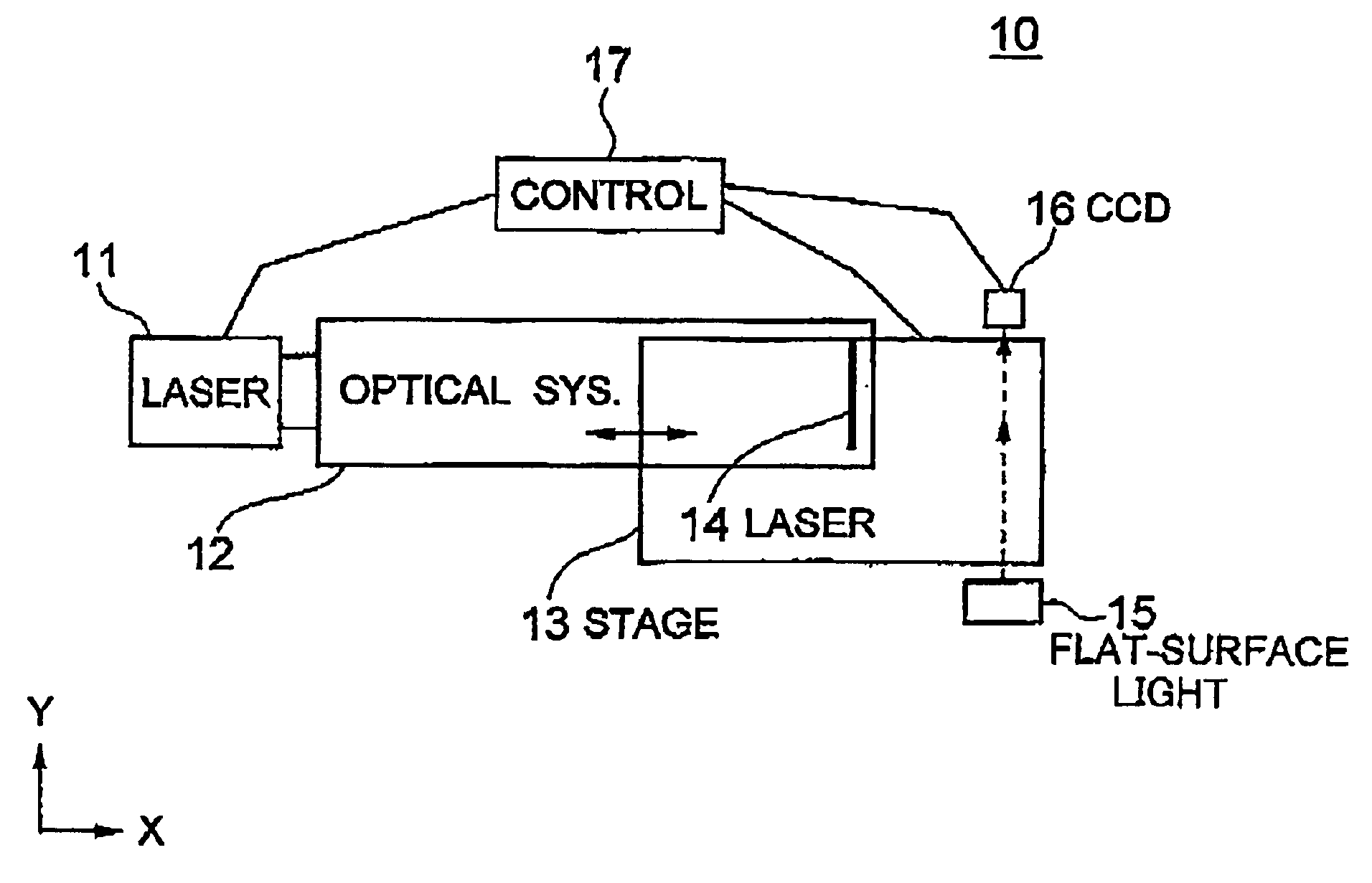
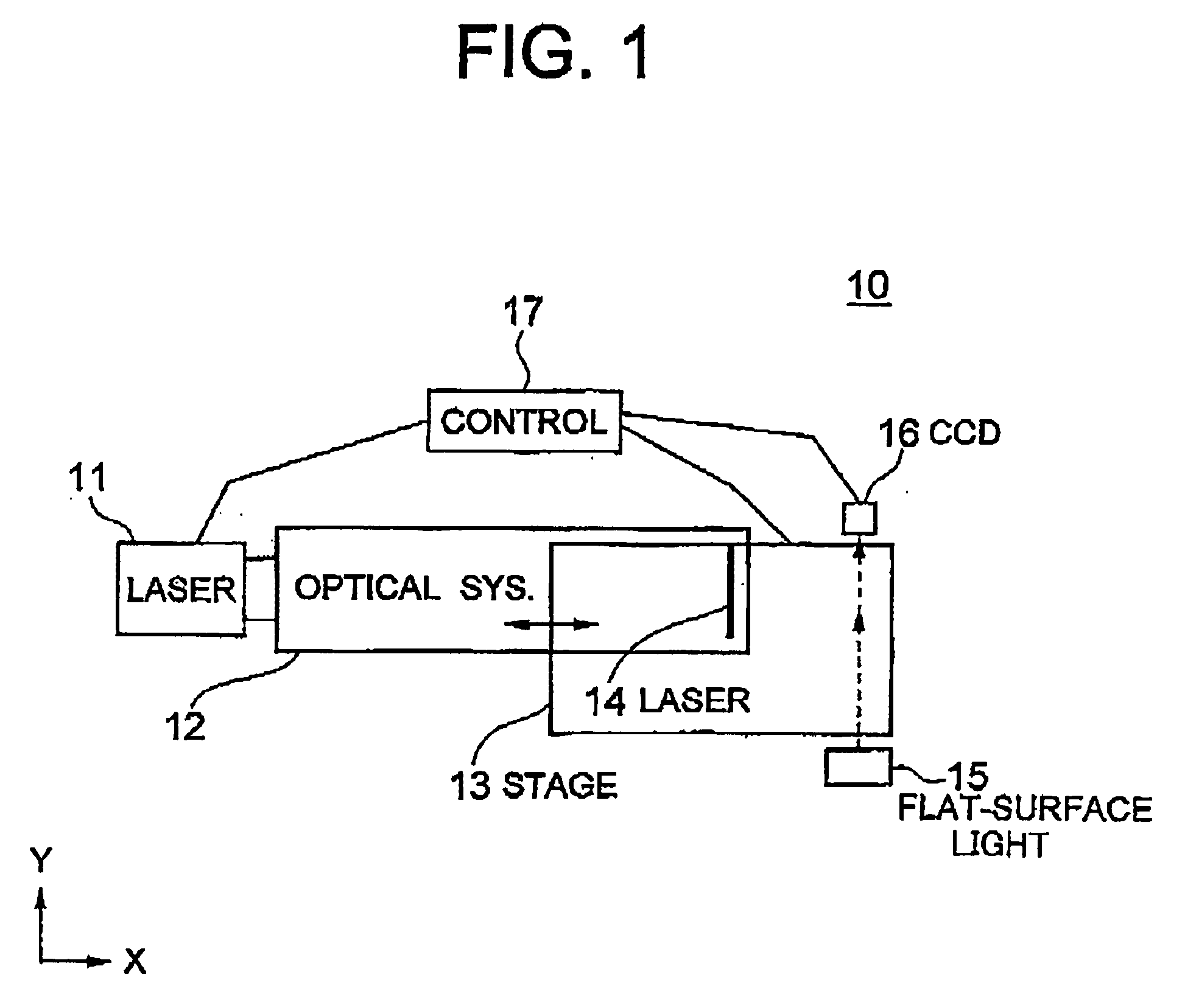
[0059] A laser irradiation apparatus according to the present invention has a structure to similar that of the laser irradiation apparatus of the first embodiment, except that the optical resolution of the CCD light-sensitive element 16 in the second embodiment is coarser than the width of the portion of the coarse crystal grains in the scanning directions. The optical resolution of the CCD light-sensitive element 16, which is coarser than the width of the portion of the coarse crystal grains in the scanning direction, does not allow the color changes between the micro-crystallized portions and portions of the coarse crystal grains to be distinguished clearly based on the image obtained by receiving the reflected light from the irradiated area. That is, substantially only colors of the micro-crystallized portions are detected.

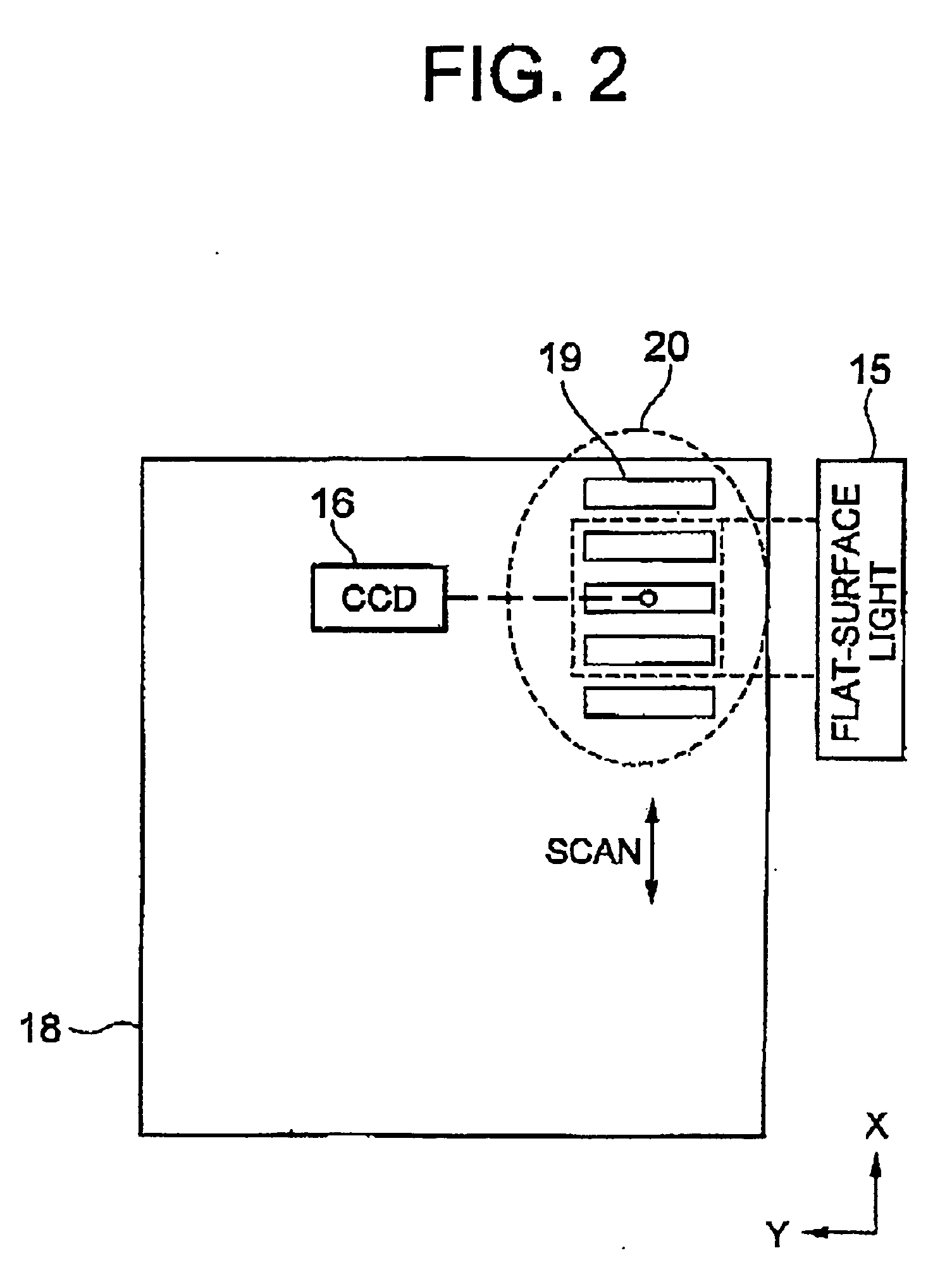
[0060]FIG. 7 shows changes in luminance of the reference color of the light received by the CCD light-sensitive element 16. For achieving the state shown by gr...


PUM

PropertyMeasurementUnit
grain diameteraaaaaaaaaa
sizeaaaaaaaaaa
sizeaaaaaaaaaa

Abstract

A method for changing an amorphous silicon film to a poly-crystalline silicon film includes the steps of irradiating an elongate pulse laser beam onto the silicon film while scanning in the direction normal to the major axis of the elongate pulse laser beam, to form a plurality of irradiated areas, irradiating flat-surface light onto the irradiated areas in the direction parallel to the major axis, and analyzing distribution of the reflected light from the irradiated areas to determine the threshold value of micro-crystallization. The threshold value is used to further determine an energy density of the elongate pulse laser beam for the phase change process.

Description

TECHNICAL FIELD [0001] The present invention relates to a laser irradiation method and a laser irradiation apparatus, and more specifically, to a laser irradiation method adopted in a laser annealing process to form a polycrystalline silicon (poly-Si) thin film by irradiating a laser beam on to a silicon film, and a laser irradiation apparatus adopting such a laser irradiation method. BACKGROUND ART [0002] In recent years, as a thin-film device to form an integrated circuit on a glass substrate, poly-Si TFTs (thin film transistors) have been vigorously developed. The poly-Si film is generally formed in an excimer laser crystallization technique. In this technique, an amorphous silicon (a-Si) film is once formed, and an excimer laser beam is irradiated onto the a-Si film to melt and re-crystallize the a-Si film, to obtain the poly-Si m In the excimer laser crystallization technique, the molten state of the a-Si film depends on the film thickness thereof, optical constant of the film,...

Claims


Application Information

Patent Timeline
Patent Type & Authority Applications(United States)
IPC IPC(8): H01L21/66B23K26/08
CPCH01L21/02678H01L27/1285H01L22/12H01L21/02691B60B21/10B60C17/066
Inventor OKUMURA, HIROSHI
Owner VISTA PEAK VENTURES LLC
Why Eureka
Try Eureka