Semiconductor device and production method thereof

a technology of semiconductor layer and semiconductor film, which is applied in the direction of semiconductor layer, semiconductor device, electrical apparatus, etc., can solve the problems of large gate leakage current generation, insufficient gate leakage current, and insufficient interface characteristics between the gate insulating film and the gan semiconductor layer, so as to reduce the gate leakage current and good interface

Inactive Publication Date: 2006-09-07
FUJITSU LTD
View PDF18 Cites 55 Cited by
  • Summary
  • Abstract
  • Description
  • Claims
  • Application Information

AI Technical Summary

Benefits of technology

[0017] According to the present invention, it is possible to provide a semiconductor device formed from a III-V nitride family semiconducto

Problems solved by technology

However, with the height of the Schottky barrier being from 1 V to 1.2 V during operations at high input power and high voltages, a large gate leakage current is generated.
However, in the

Method used


Image

  • Semiconductor device and production method thereof
  • Semiconductor device and production method thereof
  • Semiconductor device and production method thereof

Examples


first embodiment

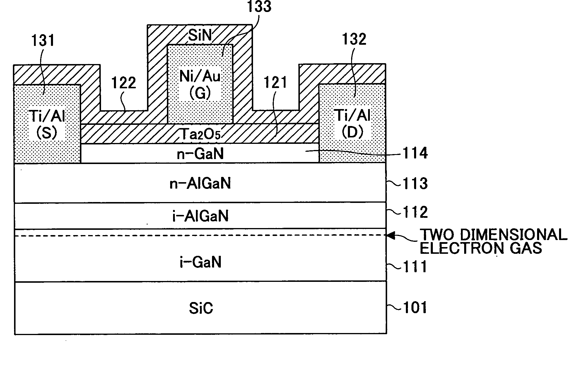
[0031]FIG. 1 is a cross-sectional view illustrating a semiconductor device formed from a III-V nitride family semiconductor according to a first embodiment of the present invention.

[0032] In the first embodiment, a HEMT (High Electron Mobility Transistor) is used as an example of a FET formed from the GaN-based semiconductor, and the HEMT includes a channel layer formed from GaN, and a carrier supplying layer formed from AlGaN.

[0033] The semiconductor device illustrated in FIG. 1 includes a substrate 101, semiconductor layers 111 through 114, a gate insulating film 121 formed on the semiconductor layers 111 through 114, an insulating film 122 formed on the surface of the gate insulating film 121, a source electrode 131, a drain electrode 132, and a gate electrode 133 formed on the gate insulating film 121. Near the surface of the semiconductor layer 111 there exists a two-dimensional electron gas.

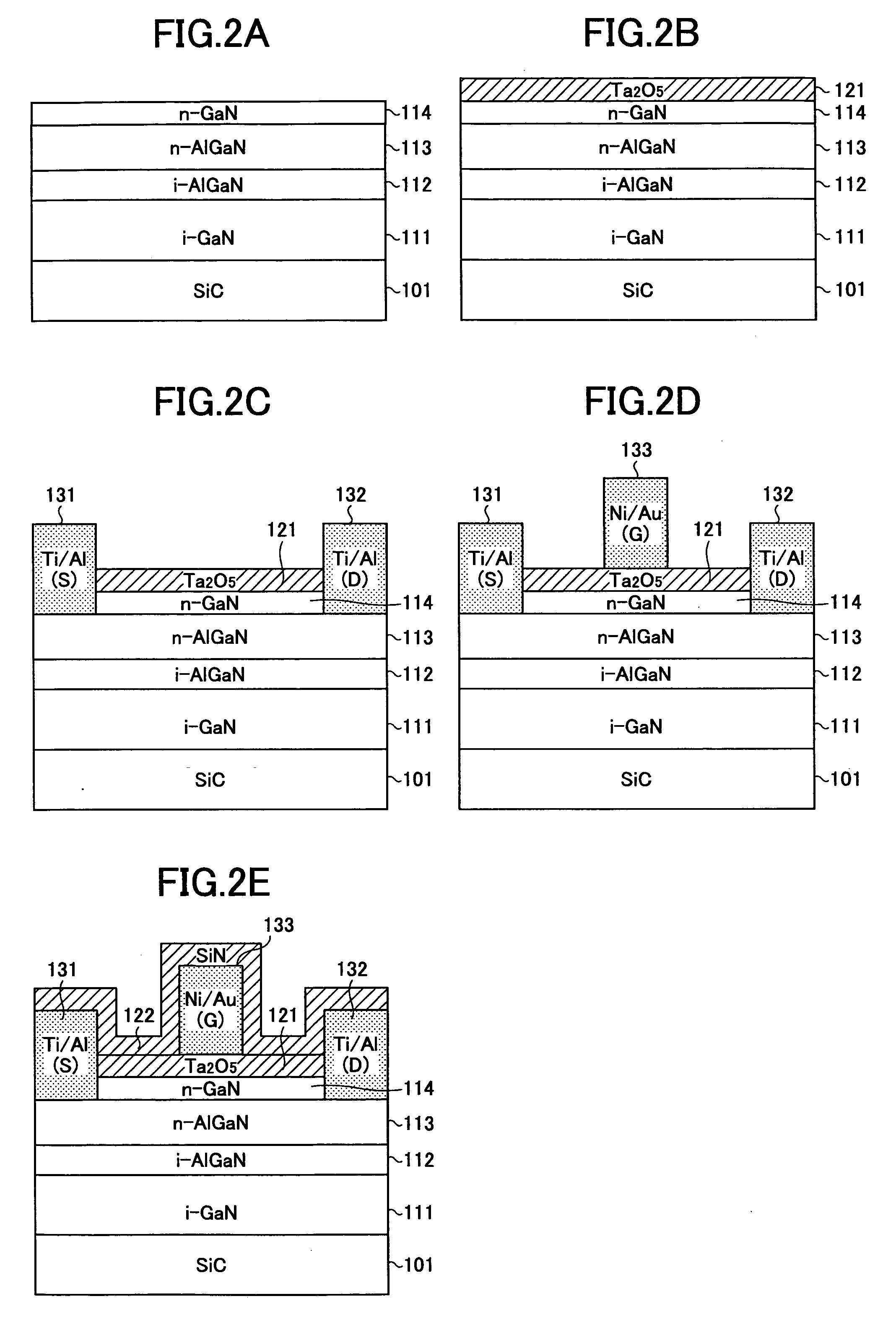
[0034]FIG. 2A through 2E are cross-sectional views illustrating a method of fabricat...

second embodiment

[0042]FIG. 3 is a cross-sectional view illustrating a semiconductor device formed from a III-V nitride family semiconductor according to a second embodiment of the present invention.

[0043] In the second embodiment, a HEMT (High Electron Mobility Transistor) is used as an example of a FET formed from the GaN-based semiconductor, and the HEMT includes a channel layer formed from GaN, and a carrier supplying layer formed from AlGaN.

[0044] The semiconductor device illustrated in FIG. 3 includes a substrate 101, semiconductor layers 111 through 114, a gate insulating film 121 formed on the semiconductor layers 111 through 114, an insulating film 122 formed on the surface of the gate insulating film 121, a source electrode 131, a drain electrode 132, and a gate electrode 133 formed on the gate insulating film 121.

[0045] The semiconductor device of the second embodiment is different from that of the first embodiment in that the gate insulating film 121 only partially covers the surface ...


PUM


Abstract

A semiconductor device formed from a III-V nitride family semiconductor is disclosed that has a reduced gate leakage current and good interface characteristics between the III-V nitride family semiconductor and a gate insulating film. The semiconductor device includes a semiconductor layer formed from the III-V nitride family semiconductor, a gate insulating film on the semiconductor layer, and a gate electrode on the gate insulating film. The gate insulating film is formed from one of a tantalum oxide, a hafnium oxide, a hafnium aluminum oxide, a lanthanum oxide, and a yttrium oxide.

Description

CROSS-REFERENCE TO RELATED APPLICATION [0001] This patent application is based on Japanese Priority Patent Application No. 2005-059380 filed on Mar. 3, 2005, the entire contents of which are hereby incorporated by reference. BACKGROUND OF THE INVENTION [0002] 1. Field of the Invention [0003] The present invention relates to a semiconductor device formed from a III-V nitride family semiconductor, such as a GaN-based semiconductor, and a method of producing the semiconductor device. [0004] 2. Description of the Related Art [0005] In recent and continuing years, study and research are being actively performed on FETs (Field Effect Transistors) formed from GaN-based semiconductors. For example, reference can be made to Japanese Laid Open Patent Application No. 2002-359256 (referred to as “reference 1”, below). The GaN-based semiconductors have features of large band-gaps, high breakdown electrical field strength, large saturation electron velocity, and other. For these reasons, it is ex...

Claims


Application Information

Patent Timeline
IPC IPC(8): H01L29/739
CPCH01L29/2003H01L29/517H01L29/7787
Inventor KANAMURA, MASAHITOOHKI, TOSHIHIRO
Owner FUJITSU LTD
Why Eureka
Try Eureka