
Non-volatile memory cells, memory arrays including the same and methods of operating cells and arrays

a non-volatile memory and array technology, applied in the field of semiconductor devices, can solve the problems of reliability problems, data retention is usually poor, and the thickness of the tunnel oxide layer may affect the channel erase speed, and achieve the effect of facilitating self-converging erase operations

Active Publication Date: 2006-09-14
MACRONIX INT CO LTD
View PDF75 Cites 139 Cited by
  • Summary
  • Abstract
  • Description
  • Claims
  • Application Information

AI Technical Summary

Benefits of technology

The present invention relates to non-volatile memory devices that have a tunnel dielectric structure that facilitates self-converging erase operations while maintaining charge retention in a charge storage layer during retention states. The tunnel dielectric structure has multiple layers with a small hole-tunneling barrier height, which allows for improved erase speeds, improved charge retention, and larger windows of operation. The memory devices in accordance with the present invention exhibit significantly improved operational properties including increased erase speeds, improved charge retention, and larger windows of operation. The methods of operation in accordance with the present invention include applying self-converging reset / erase voltages to the substrate and the gate electrode in each memory cell, programming at least one of the memory cells, and reading at least one of the memory cells by applying a voltage between an erased state level and a programmed state level of at least one of the memory devices. The present invention also includes methods of forming a memory cell, which involve providing a semiconductor substrate, forming a tunnel dielectric structure, forming a charge storage layer, forming an insulating layer, and forming a gate electrode.

Problems solved by technology

Although such designs may have good erase speed, the data retention is usually poor, in part because direct tunneling may occur even at a low electrical field strengths that may exist during a retention state of a memory device.
However, a thick tunnel oxide layer may impact channel erase speed.
However, the BTBTHH erase methods may cause some reliability issues.
For example, the characteristics of NROM devices employing BTBTHH erase methods may degrade after numerous P / E (program / erase) cycles.

Method used


Image

  • Non-volatile memory cells, memory arrays including the same and methods of operating cells and arrays
  • Non-volatile memory cells, memory arrays including the same and methods of operating cells and arrays
  • Non-volatile memory cells, memory arrays including the same and methods of operating cells and arrays

Examples


Embodiment Construction

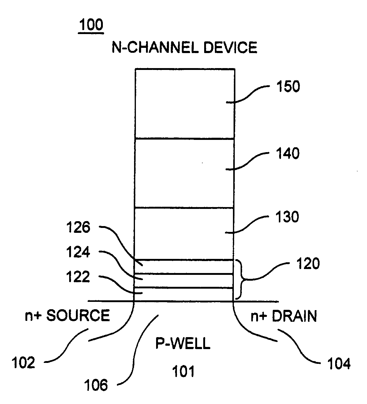
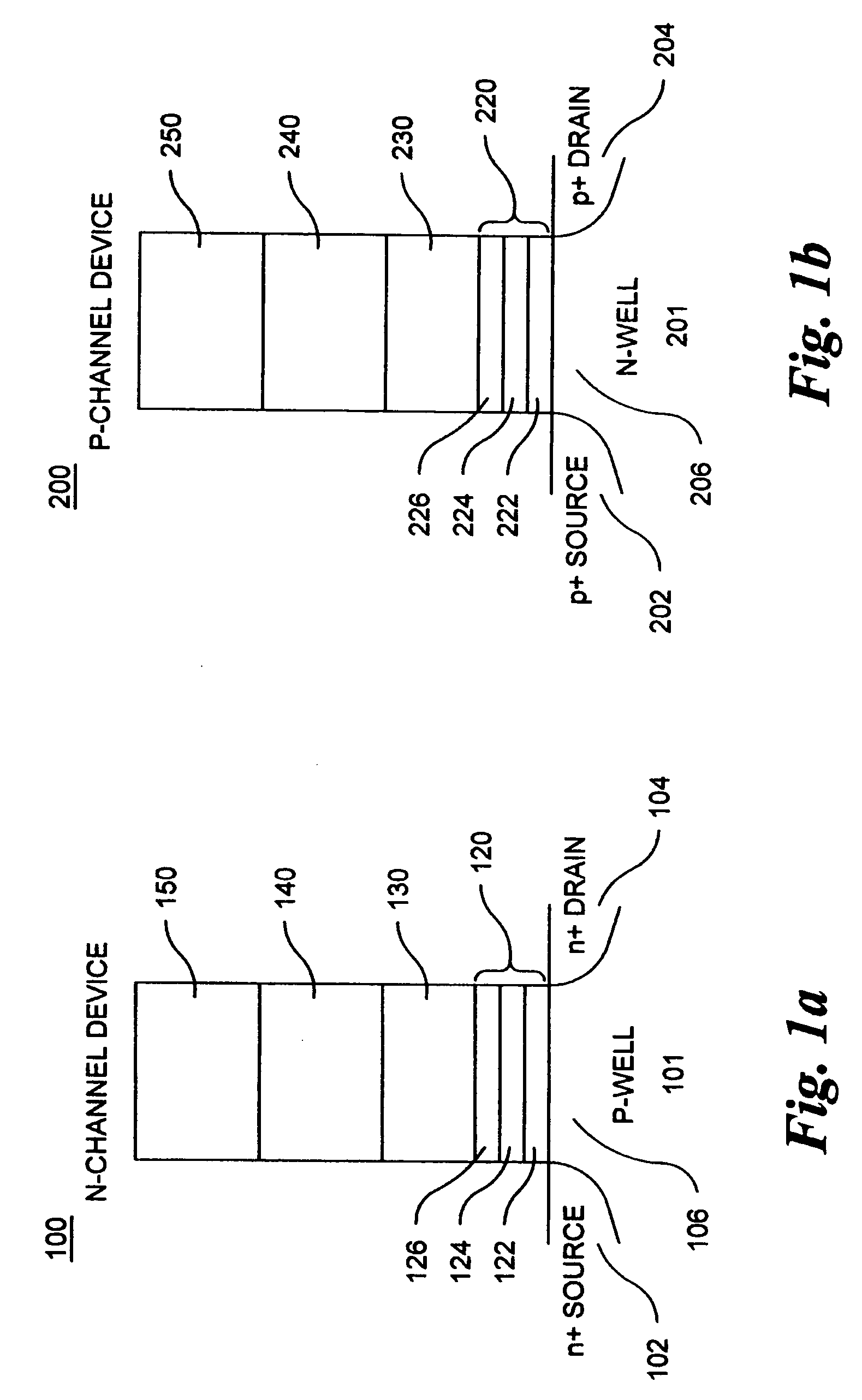
[0054] Reference will now be made in detail to the invention and the presently preferred embodiments thereof, examples of which are illustrated in the accompanying drawings. Wherever possible, the same or similar reference numbers are used in the drawings and the description to refer to the same or like parts. It should be noted that the non-graph drawings are in greatly simplified form and are not to precise scale. In reference to the disclosure herein, for purposes of convenience and clarity only, directional terms, such as top, bottom, left, right, up, down, above, below, beneath, rear, and front, are used with respect to the accompanying drawings. Such directional terms used in conjunction with the following description of the drawings should not be construed to limit the scope of the invention in any manner not explicitly set forth in the appended claims. Although the disclosure herein refers to certain illustrated embodiments, it is to be understood that these embodiments are ...


PUM


Abstract

Memory cells comprising: a semiconductor substrate having a source region and a drain region disposed below a surface of the substrate and separated by a channel region; a tunnel dielectric structure disposed above the channel region, the tunnel dielectric structure comprising at least one layer having a small hole-tunneling-barrier height; a charge storage layer disposed above the tunnel dielectric structure; an insulating layer disposed above the charge storage layer; and a gate electrode disposed above the insulating layer are described along with arrays thereof and methods of operation.

Description

CROSS-REFERENCE TO RELATED APPLICATIONS [0001] This application is based upon, and claims priority under 35 U.S.C. § 119(e) of: provisional U.S. patent application Ser. No. 60 / 640,229, filed on Jan. 3, 2005; provisional U.S. patent application No. 60 / 647,012, filed on Jan. 27, 2005; provisional U.S. patent application Ser. No. 60 / 689,231, filed on June 10, 2005; and provisional U.S. patent application Ser. No. 60 / 689,314, filed on Jun. 10, 2005; the entire contents of each of which are incorporated herein by reference.BACKGROUND OF THE INVENTION [0002] Non-volatile memory (“NVM”) refers to semiconductor memory which is able to continually store information even when the supply of electricity is removed from the device containing the NVM cell. NVM includes Mask Read-Only Memory (Mask ROM), Programmable Read-Only Memory (PROM), Erasable Programmable Read-Only Memory (EPROM), Electrically Erasable Programmable Read-Only Memory (EEPROM), and Flash Memory. Non-volatile memory is extensiv...

Claims


Application Information

Patent Timeline
Patent Type & Authority Applications(United States)
IPC IPC(8): H01L29/792
CPCG11C16/0475G11C16/0483G11C16/0491H01L27/115H01L27/11568H01L29/66833H01L29/792H10B43/30H10B69/00
Inventor LUE, HANG-TINGWANG, TZU YU
Owner MACRONIX INT CO LTD
Learn More