Wireless chip and electronic appliance having the same
- Summary
- Abstract
- Description
- Claims
- Application Information
AI Technical Summary
Benefits of technology
Problems solved by technology
Method used
Image

Examples
embodiment mode 1
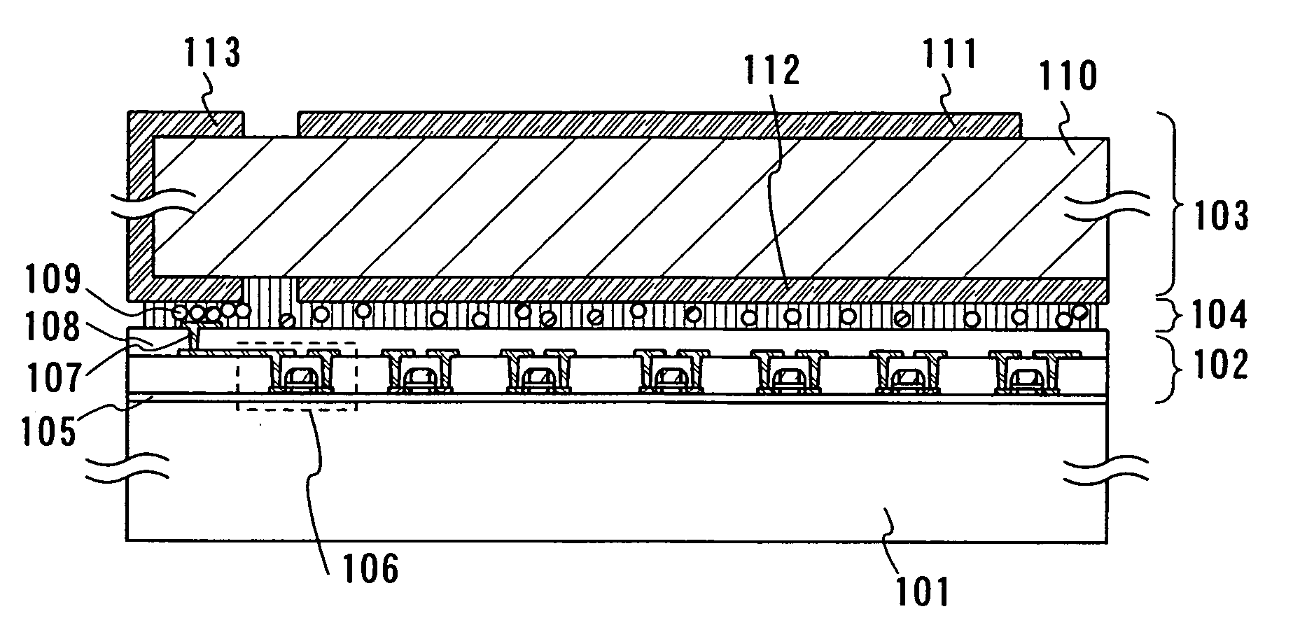
[0051] An embodiment mode of a wireless chip of the present invention is shown in FIGS. 1A and 1B. FIGS. 1A and 1B are cross-sectional views of a wireless chip.
[0052] In a wireless chip of this embodiment mode, a layer 102 having a thin film transistor formed over an insulating substrate 101 is fixed to an antenna 103 by an anisotropic conductive adhesive 104. Moreover, a connection terminal 107 of the layer 102 having a thin film transistor and a power feeding layer 113 of the antenna are electrically connected by conductive particles 109 dispersed in the anisotropic conductive adhesive 104. Further, although not shown, a ground wiring of the layer having a thin film transistor is electrically connected to a conductive layer serving as a ground contact body of the antenna.
[0053] As the insulating substrate 101, an inflexible insulating substrate is preferred. A quartz substrate or a glass substrate such as a nonalkali glass substrate is used.
[0054] The layer 102 having a thin fi...
embodiment mode 2
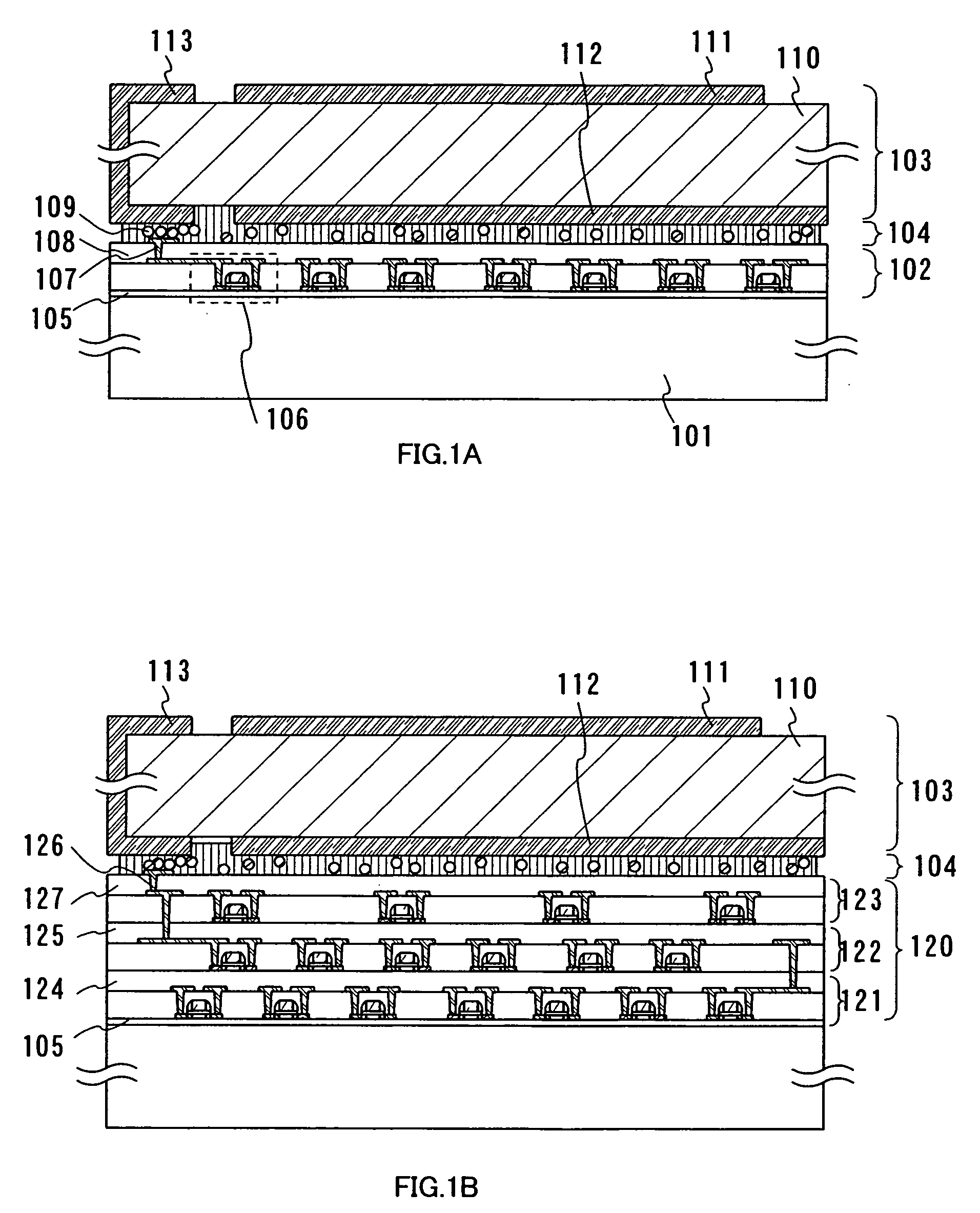
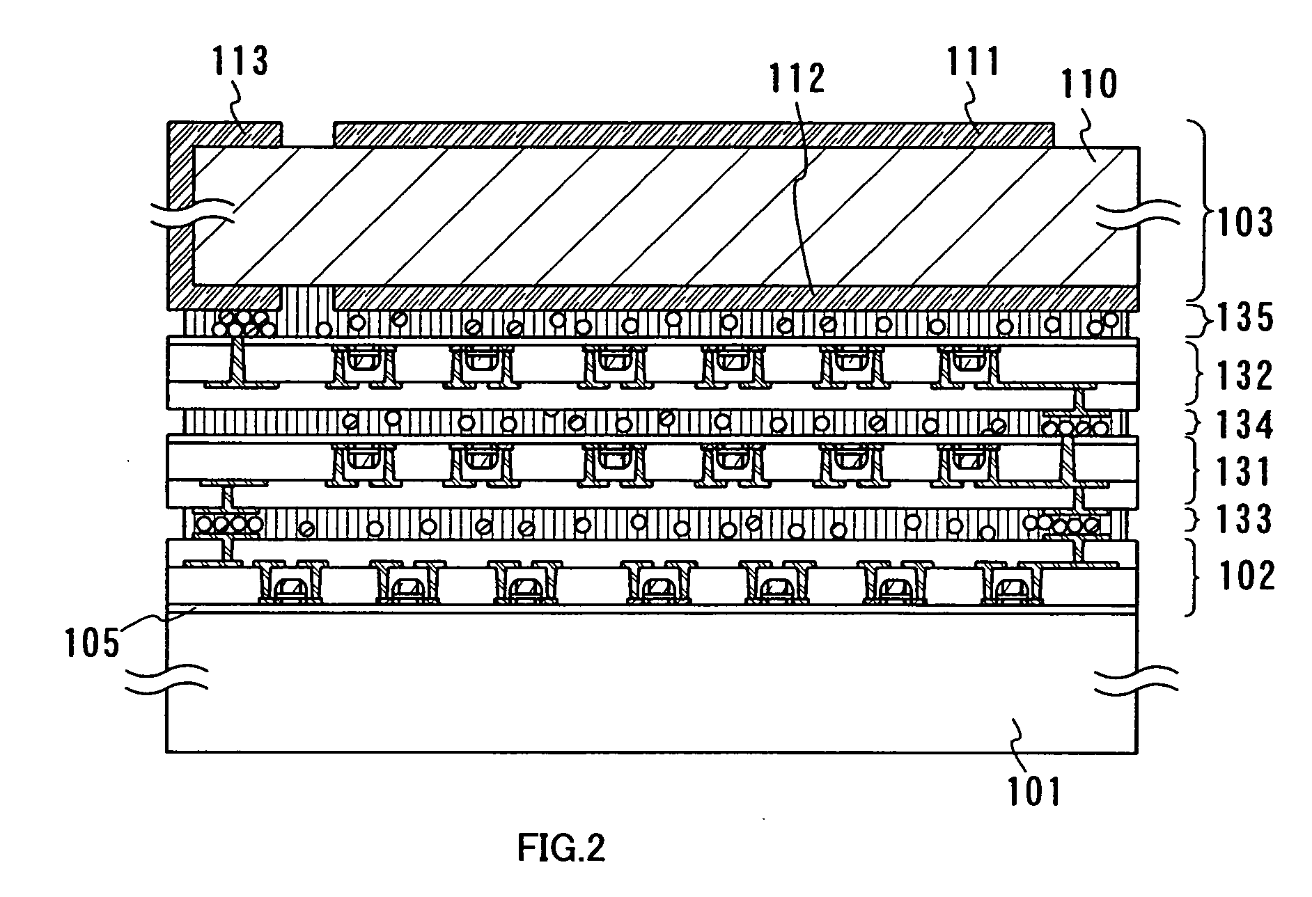
[0117] An embodiment mode of a wireless chip of the present invention is shown in FIG. 2. FIG. 2 is a cross-sectional view of a wireless chip. In this embodiment mode, a structure of a wireless chip which has a patch antenna and plural layers having thin film transistors wherein the layers are fixed to each other by an anisotropic conductive adhesive is described.
[0118] In a wireless chip of this embodiment mode, a first layer 102 having a thin film transistor is formed over an insulating substrate 101 similarly to Embodiment Mode 1. Further, the first layer 102 having a thin film transistor and a second layer 131 having a thin film transistor are fixed to each other by an anisotropic conductive adhesive 133.
[0119] A first connection terminal formed on the surface of the first layer 102 having a thin film transistor is electrically connected to a second connection terminal formed on the surface of the second layer having a thin film transistor through conductive particles disperse...
embodiment mode 3
[0129] An embodiment mode of a wireless chip of the present invention will be described with reference to FIG. 3. FIG. 3 is a cross-sectional view of a wireless chip. This embodiment mode will describe a structure of a wireless chip in which a layer having a thin film transistor and a patch antenna are provided in different regions over an insulating substrate.
[0130] Over the insulating substrate 101, a layer 141 having a thin film transistor is formed in a first region 145. On a surface of the layer 141 having a thin film transistor, a connection terminal 143 is formed. The layer 141 having a thin film transistor can be formed similarly to the first layer 102 having a thin film transistor in Embodiment Mode 1. Further, as shown in FIG. 3, parts of the thin film transistor and the insulating layer formed thereover that are in a second region 146 may be removed.
[0131] The antenna 103 is fixed onto the second region 146 by an anisotropic conductive adhesive 142. The connection termi...
PUM
 Abstract
Description
Claims
Application Information