Method for producing a semiconductor device and resulting device

Active Publication Date: 2006-09-14
INTERUNIVERSITAIR MICRO ELECTRONICS CENT (IMEC VZW)
View PDF12 Cites 50 Cited by
  • Summary
  • Abstract
  • Description
  • Claims
  • Application Information

AI Technical Summary

Benefits of technology

[0036] An advantage of the present invention is that the active side of the semiconductor device is protected and remains essentially unaffected. A further advantage is that the resulting structure is more compact, compared to devices produced by applying air bridge structures. The device produced according to the present invention is highly integrated, has short interconnects and a planar character, allowing further 3D integration.
[0037] In a second embodiment, the method comprises a number of further steps, following the steps of the first embodiment. After the connection between the source/gate/drain structures has been established, the second substrate, which is now carrying the finished interconnected device, may be reversed and attached to a third substrate, by attaching the side of the second substrate, carrying the interconnect layer, to the third substrate, preferably an MCM substrat

Problems solved by technology

High frequency and power devices are generally confronted by a problem of thermal management.
This however results in a device with a considerab

Method used


Image

  • Method for producing a semiconductor device and resulting device
  • Method for producing a semiconductor device and resulting device
  • Method for producing a semiconductor device and resulting device

Examples


first embodiment

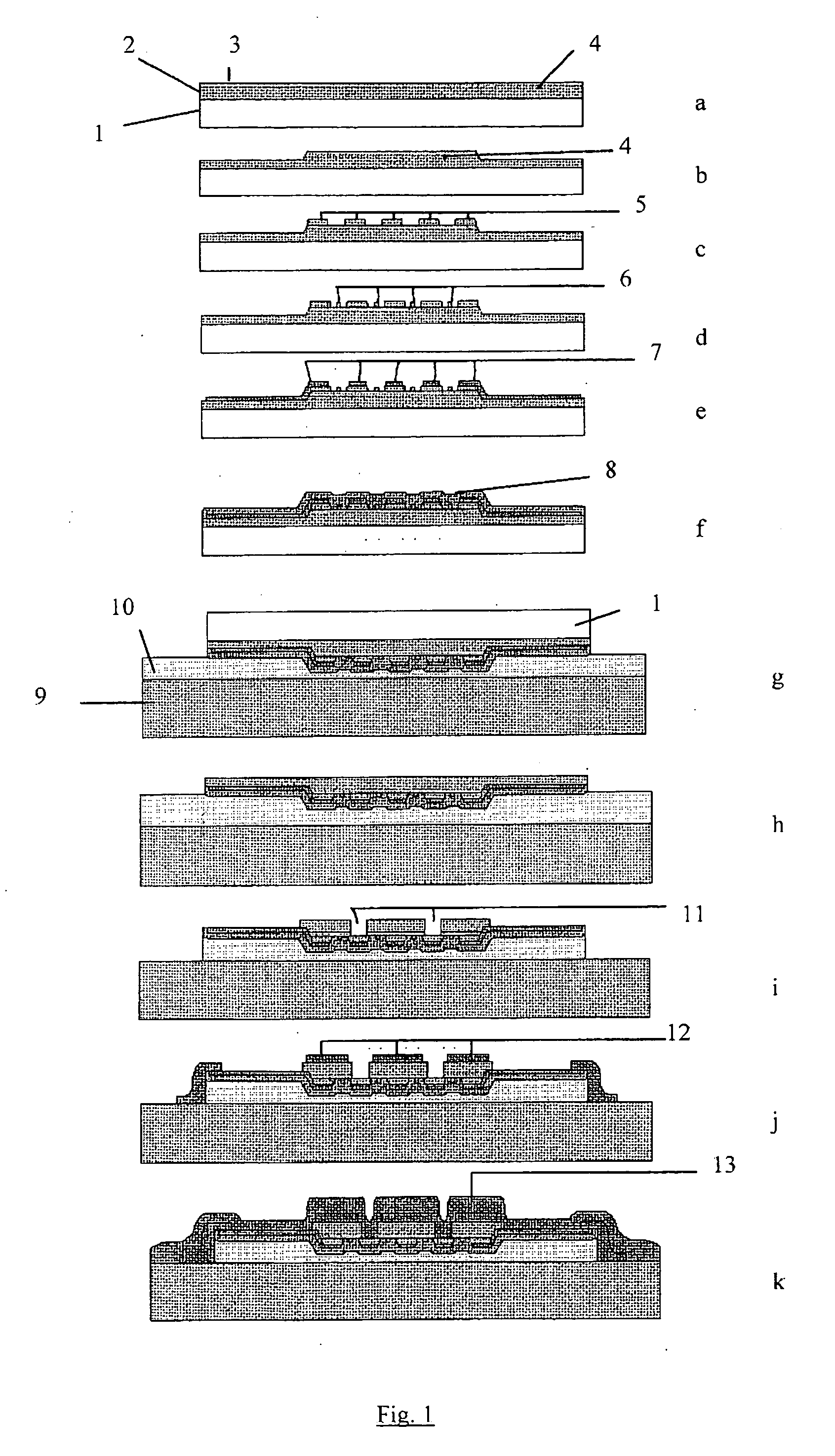
[0056] The preferred embodiment of the present invention concerns the production of a multi-finger HEMT device according to the method as characterised above. In FIG. 1, the different process steps of producing a HEMT according to the invention, are illustrated. The steps will be further highlighted hereafter.

[0057]FIG. 1a: providing a sapphire substrate 1, with a semiconductor stack on top of it. The stack consists of a GaN layer 2 and an AlGaN layer 3. The GaN film is between 1 and 5 μm thick and grown on the sapphire substrate in a MOCVD system (Metal Organic Chemical Vapour Deposition). The top layer 3 of AlGaN (15-30 nm) film is grown on top such that a high concentration of electrons occurs at the interface (two dimensional electron gas, 2-DEG).

[0058]FIG. 1b: a mesa etch is done to isolate individual devices on the substrate. The etch has to go through the 2-DEG interface 4.

[0059]FIG. 1c: A metal stack 5 is deposited for the drain and source contacts. The source and drain co...

second embodiment

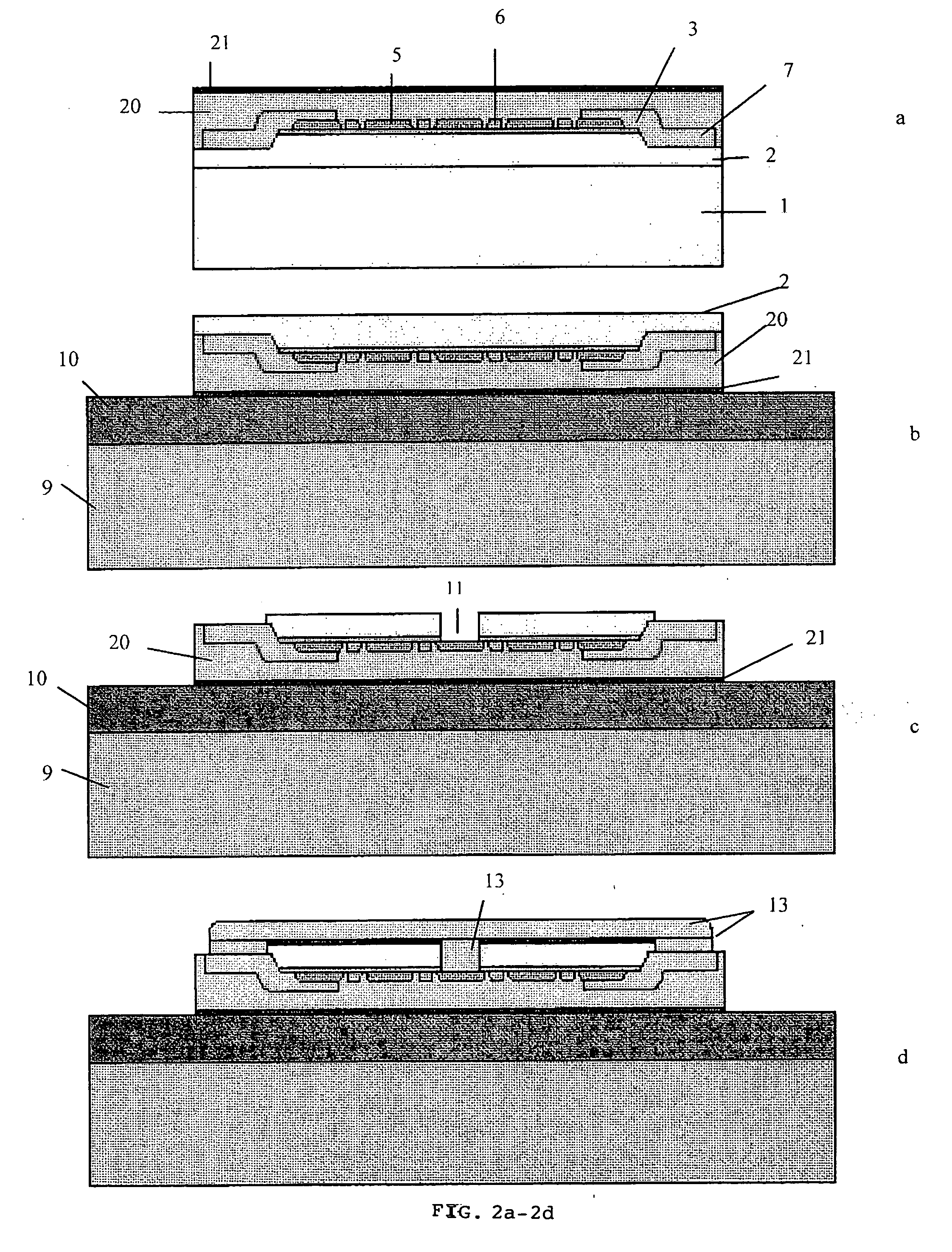
[0074] a number of additional steps are performed, as illustrated in FIG. 2.

[0075]FIG. 2a: The same steps as desbribed above are applied to obtain the gate source and drain contact zones 5 and 6 on the substrate 1. A passivation layer 20 is deposited on the contacts 5 and 6, with an etch stop 21 layer on top of the passivation layer.

[0076]FIG. 2b: the substrate 1 is reversed and bonded to the second substrate 9, after which the first substrate 1 is removed, in the same way as in the first embodiment. The bonding layer 10 according to this embodiment is not necessarily a thermally conductive adhesive layer. It may be SU8 / BCB or metal.

[0077]FIG. 2c: vias 11 are etched to the contact areas. In principle, vias to only the source contacts would be enough in this case, but the disadvantage here then is that the devices cannot be measured before bonding to the third substrate. In the preferred case of this embodiment, therefore, vias are produced to all contact areas (source, drain, gat...

embodiment 1

[0089]FIGS. 7a and 7b show two possibilities which can be used in a device according to The interconnect layer 13 shows three distinct regions, and thus allows a common contact to the gates, drains and sources respectively.


PUM


Abstract

The present invention is related to a method of producing a semiconductor device and the resulting device. The method is suitable in the first place for producing high power devices, such as High Electron Mobility Transistors (HEMT), in particular HEMT-devices with multiples source-gate-drain groups or multiple base bipolar transistors. According to the method, the interconnect between the source contacts is not produced by air bridge structures, but by etching vias through the semiconductor layer directly to the ohmic contacts and applying a contact layer on the backside of the device.

Description

RELATED APPLICATIONS [0001] This application claims the benefit under 35 U.S.C. § 119(e) of U.S. Patent Application No. 60 / 648,841 filed Jan. 31, 2005 for “INTEGRATION OF POWER HEMT'S”, and claims the benefit under 35 U.S.C. § 119(a) of European Patent Application No. EP 05447156 filed on Jun. 30, 2005, all of which are hereby incorporated by reference.BACKGROUND OF THE INVENTION [0002] 1. Field of the Invention [0003] The present invention is related to semiconductor devices comprising multiple source-gate-drain combinations, in particular devices that are designed to work at high frequency and high power levels, such as multiple gate-finger High Electron Mobility Transistors (HEMTs), i.e. having at least two gate contacts on the same substrate. [0004] 2. Description of the Related Art [0005] High frequency and power devices are generally confronted by a problem of thermal management. In HEMT-devices, heat is generated in a very small area, especially in the channel, close to the g...

Claims


Application Information

Patent Timeline
IPC IPC(8): H01L21/336
CPCH01L29/42316H01L29/66462H01L2924/12042H01L2924/1305H01L2924/15788H01L2924/13064H01L2924/01041H01L2924/01023H01L2924/01006H01L2221/68363H01L2224/24226H01L2924/01013H01L2924/01029H01L2924/01032H01L2924/01033H01L2924/0104H01L2924/01042H01L2924/01046H01L2924/0106H01L2924/01073H01L2924/01074H01L2924/01078H01L2924/01079H01L2924/01082H01L2924/10329H01L2924/1423H01L2924/19041H01L2924/19043H01L21/6835H01L23/373H01L24/24H01L24/82H01L29/41725H01L2924/01005H01L2924/00H01L29/4175H01L29/41758
Inventor DAS, JOHANRUYTHOOREN, WOUTER
Owner INTERUNIVERSITAIR MICRO ELECTRONICS CENT (IMEC VZW)
Why Eureka
Try Eureka