Method for Etching Microchannel Networks within Liquid Crystal Polymer Substrates

a technology of liquid crystal polymer substrates and microchannel networks, which is applied in the direction of etching metal masks, crystal growth processes, lithographic masks, etc., can solve the problems of increasing the cost of finer dimensional control, increasing the cost of electrical circuits, and warranting the increase of the cost associated with their manufactur

Inactive Publication Date: 2006-09-28
UNIV OF SOUTH FLORIDA
View PDF10 Cites 6 Cited by
  • Summary
  • Abstract
  • Description
  • Claims
  • Application Information

AI Technical Summary

Benefits of technology

[0023] The present invention provides many advantages over the prior art, including the ability to create channels and conduits in 3-D dimensions, not limited to 1-D surface features or 2-D voids, vias or thru-holes.
[0024] The present invention provides horizontal networks of conduits, thereby establishing a path for fluid flow in 3-D. The deep etch capabilities of the method of the present invention allows the formation of these networks.
[0025] An additional advantage of the method of the present invention also allows for the simultaneous combination of electrical structures and functions within or in proximity to the fluid channels, thereby creating fluidics alone, fluidics with electronics, embedded optical waveguides for photonics and combinations of any of the aforementioned structures.

Problems solved by technology

In addition to the increased flow resistance, at sub 30 μm dimensions, there is an increased cost for finer dimensional control.
In contrast, electrical circuits yield increased performance with smaller dimensions and warrant the increased cost associated with their manufacture.
However, to date, most of these photolithographic procedures involve multi-step mask and developing steps, thus making processing labor intensive and expensive.
However, these methods do not teach or suggest the formation of microchannels or channel-like structures that are effective in establishing electrical, optical and fluidic circuitry.
These methods do not teach or suggest the formation of channels or channel-like structures effective in establishing electrical, optical and fluidic circuitry.
These methods do not teach or suggest the use of an etchant system to form complex channels and fluid pathways necessary for the construction of an operational microfluidic device.
The methods known in the art utilizing etchants to produce incidental features in the substrate do not result in the formation of effective grooved patterns and fluid conduits in the substrate that are continuous patterns that can be used in the subsequent formation of microfluidic devices.
Although the vias and holes are formed using masking techniques known in the art, these methods do not teach or suggest a method for connecting these features together in a continuous pattern necessary to provide fluid transport.
While various means for the etching of polymer surfaces are known in the art, the current state of the art does not teach or suggest the formation of complex channel structures and other fluidic canals necessary to fabricate microfluidic devices.
In addition, all of these features are intermediate in nature, and provide little function, and do not contribute to the development of a functional pathway for the fabrication of micofluidic devices.

Method used


Image

  • Method for Etching Microchannel Networks within Liquid Crystal Polymer Substrates
  • Method for Etching Microchannel Networks within Liquid Crystal Polymer Substrates

Examples


Embodiment Construction

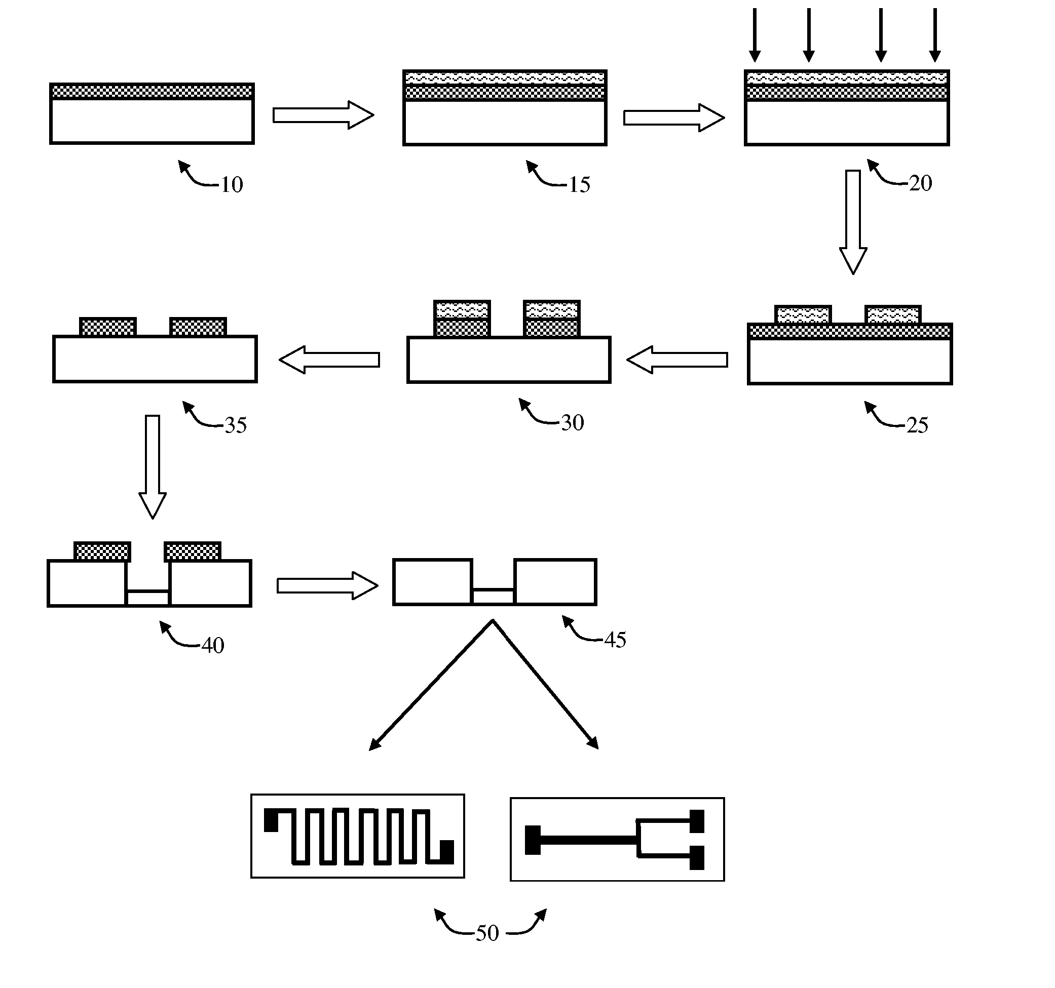
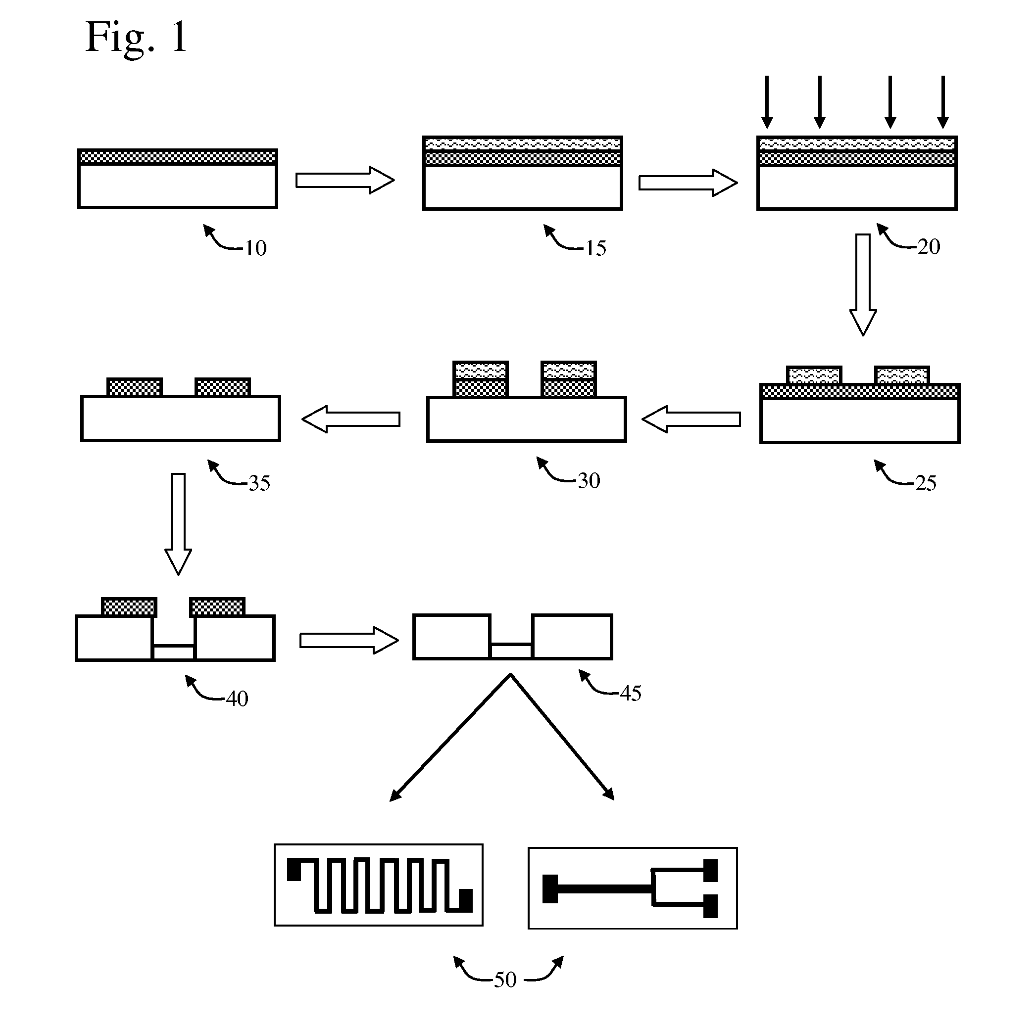
[0027] The method in accordance with the present invention is outlined as shown with reference to FIG. 1. The illustrated process of FIG. 1 demonstrates the process flow for the preparation of a microfluidic device utilizing a liquid crystal polymer (LCP) / copper laminate as the starting material in accordance with the present invention.

[0028] With reference to FIG. 1, in an exemplary embodiment the method of the present invention includes the steps of applying a copper layer to a liquid crystal polymer layer to form a copper clad liquid crystal polymer substrate 10, applying a patterned photoresist to the copper clad liquid crystal polymer substrate 15, wherein the patterned photoresist defines a desired microchannel network, exposing the patterned photoresist to a light source 20, developing the exposed patterned photoresist 25, etching the copper layer of the copper clad liquid crystal polymer substrate to expose the liquid crystal polymer layer of the substrate 30, removing the ...


PUM

PropertyMeasurementUnit
sizeaaaaaaaaaa
depthaaaaaaaaaa
liquidaaaaaaaaaa

Abstract

The present invention provides for a method for the fabrication of microchannels, and more particularly to the fabrication of microchannels for use in Microelectromechanical (MEMS) devices and MEMS related devices. In accordance with an embodiment of the present invention, microchannels are formed by a microfabrication method utilizing electronic imaging techniques in combination with chemical etching and subsequent metallization. The method of the present invention is effective in producing networks of channels in liquid crystal polymer (LCP) polymeric substrates which are highly defined in terms of their patterns, and thus are able to encompass a wide variety of end uses.

Description

CROSS REFERENCE TO RELATED APLICATIONS [0001] This application claims priority to currently pending U.S. Provisional Patent Application No. 60 / 521,756, entitled, “Method for Etching Microchannel Networks within Liquid Crystal Polymer Substrates”, filed Jun. 30, 2004.STATEMENT OF GOVERNMENT INTEREST [0002] This invention was made with Government support under Grant No. N00014-98-1-0848 awarded by the Office of Naval Research. The Government has certain rights in the invention.BACKGROUND OF INVENTION [0003] Channel architectures are almost universally found in complex natural and synthetic systems. Channels existing as waveguides, particle guides, and circuits and are found in both raised and recessed forms. Although channels can be used for theoretical illustrations, such as a channel capacity in an information system, channels are practical solutions for efficiently routing physical particles such as electrons, ions, molecules, protons, etc. from a source to a destination. [0004] Ch...

Claims


Application Information

Patent Timeline
Patent Type & Authority Applications(United States)
IPC IPC(8): G03F7/20
CPCB01L3/5027B81B1/00B81B2203/0323B81C1/00071G02B6/136H05K3/002H05K3/107H05K2201/0141H05K2201/09036H05K2203/0554
Inventor FRIES, DAVID P.STEIMLE, GEORGEBROADBENT, HEATHER
Owner UNIV OF SOUTH FLORIDA
Why Eureka
Try Eureka